What is a Tunnel Diode?
What is a Tunnel Diode?
Tunnel Diode
A tunnel diode (also known as a Esaki diode) is a type of semiconductor diode that has effectively “negative resistance” due to the quantum mechanical effect called tunneling. Tunnel diodes have a heavily doped pn junction that is about 10 nm wide. The heavy doping results in a broken band gap, where conduction band electron states on the N-side are more or less aligned with valence band hole states on the P-side.

Transistors struggle with very high frequencies due to transit time and other effects. Many devices use the negative conductance property of semiconductors for high-frequency applications. A tunnel diode, also known as an Esaki diode, is a commonly used negative conductance device named after L. Esaki for his work on tunneling.
The concentration of dopants in both p and n region is very high, at around 1024 – 1025 m-3. The pn junction is also abrupt. For this reasons, the depletion layer width is very small. In the current voltage characteristics of tunnel diode, we can find a negative slope region when a forward bias is applied.
The name “tunnel diode” is due to the quantum mechanical tunneling is responsible for the phenomenon that occurs within the diode. The doping is very high so at absolute zero temperature the Fermi levels lies within the bias of the semiconductors.
Characteristics of Tunnel Diode
When reverse bias is applied, the Fermi level of the p-side becomes higher than that of the n-side, causing electrons to tunnel from the valence band of the p-side to the conduction band of the n-side. As the reverse bias increases, the tunnel current also increases.
When forward bias is applied the Fermi level of n-side becomes higher that the Fermi level of p-side, thus the tunneling of electrons from the n-side to p-side takes place. The amount of the tunnel current is very large than the normal junction current. When the forward bias is increased, the tunnel current is increased up to certain limit.

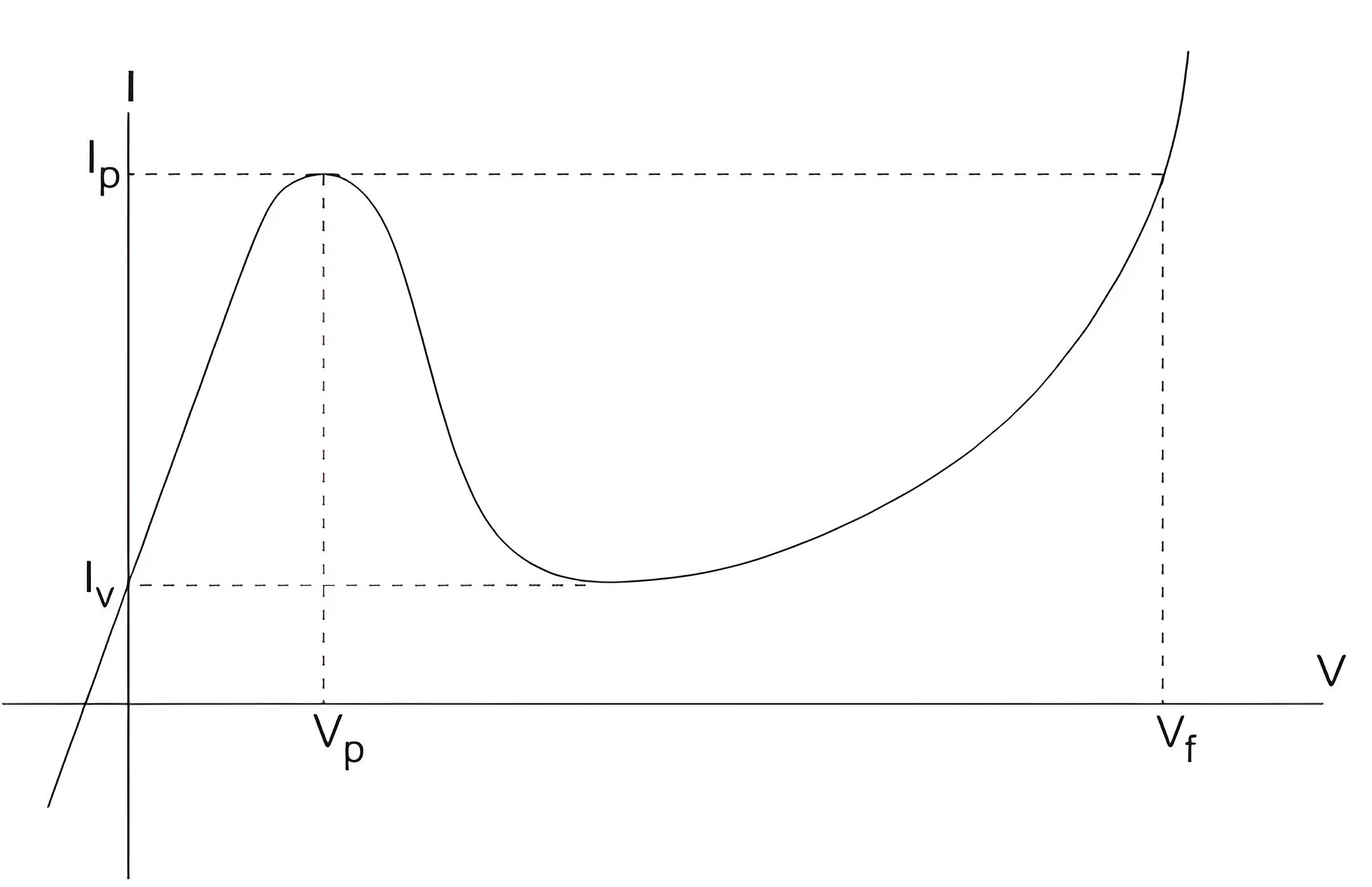
When the band edge of n-side is the same as the Fermi level in p-side, the tunnel current is maximum with the further increment in the forward bias the tunnel current decreases and we get the desired negative conduction region. When the forward bias is raised further, normal pn junction current is obtained which is exponentially proportional to the applied voltage. The V-I characteristics of the tunnel diode is given,
The negative resistance is used to achieve oscillation and often Ck+ function is of very high frequency frequencies.
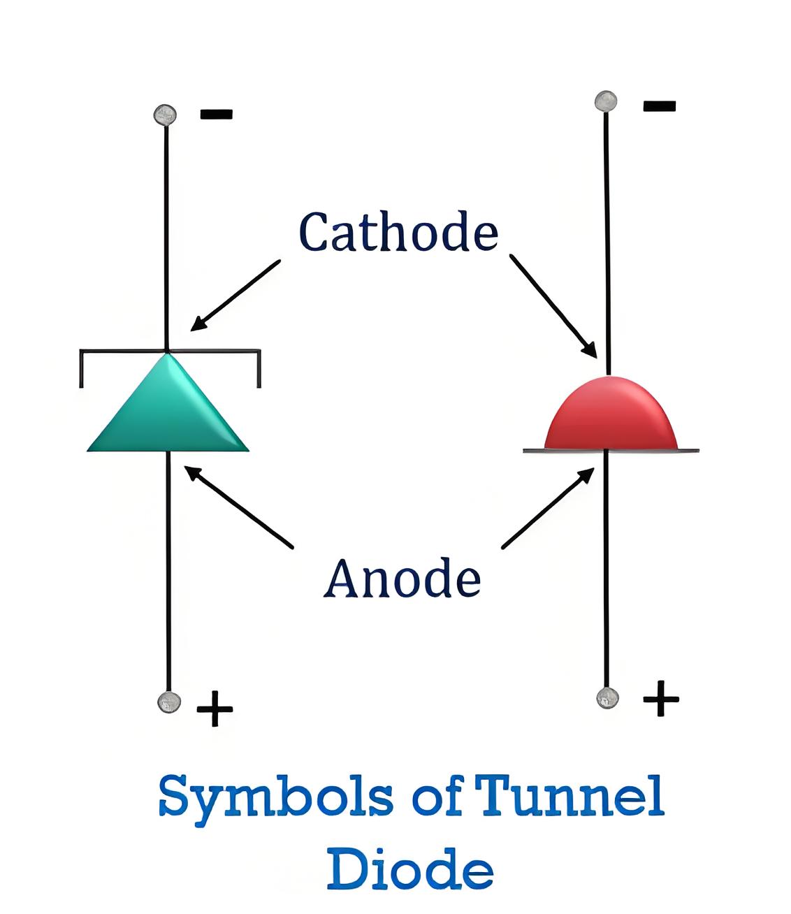
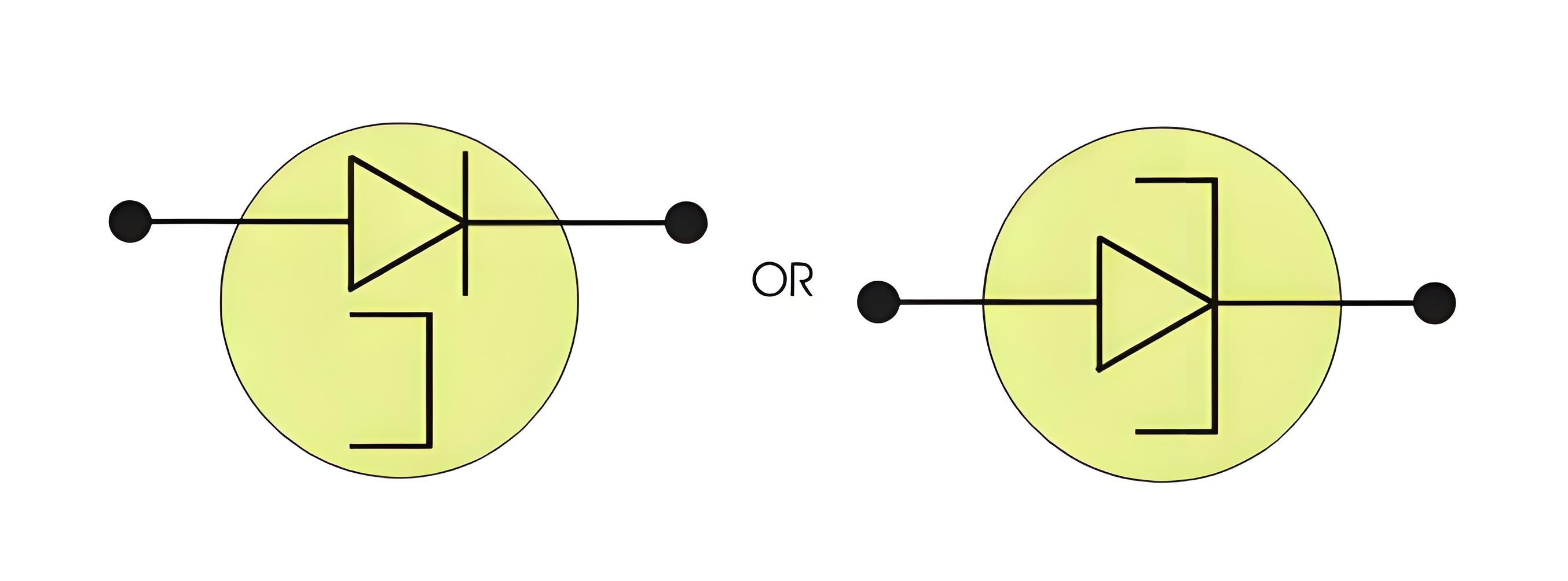
Tunnel Diode Symbol

Tunnel Diode Applications
Oscillator Circuits
Used in Microwave Circuits
Resistant to Nuclear Radiation
The Electricity Encyclopedia is dedicated to accelerating the dissemination and application of electricity knowledge and adding impetus to the development and innovation of the electricity industry.


