How Dose a Transistor Work?
How Dose a Transistor Work?
Transistor Definition
A transistor is defined as a semiconductor device used to amplify or switch electronic signals.
There are different types of transistors available, but we’ll focus on the NPN transistor in common emitter mode. This type has a heavily doped and wide emitter region, which contains many free electrons (majority carriers).
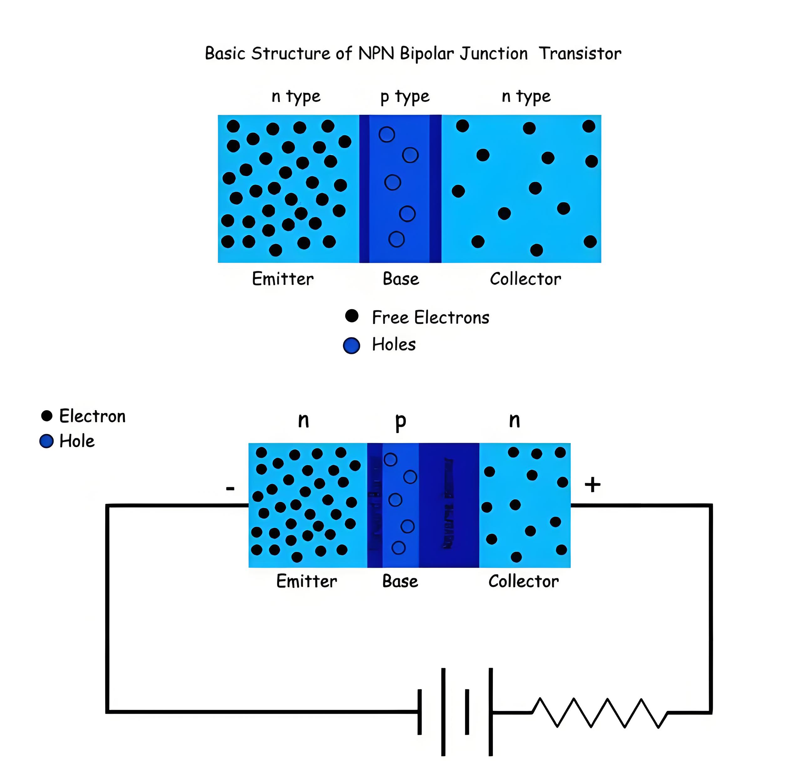
The collector region is wide and moderately doped, so it has fewer free electrons than the emitter. The base region is very thin and lightly doped, with a small number of holes (majority carriers). Now, we connect one battery in between emitter and collector. The emitter terminal of the transistor is connected to the negative terminal of the battery. Hence the emitter-base junction becomes forward biased, and base-collector junction becomes reverse biased. In this condition, no current will flow through the device. Before going to the actual operation of the device let us recall the constructional and doping details of an NPN transistor. Here the emitter region is wider and very heavily doped. Hence the concentration of majority carriers (free electrons) in this region of the transistor is very high.
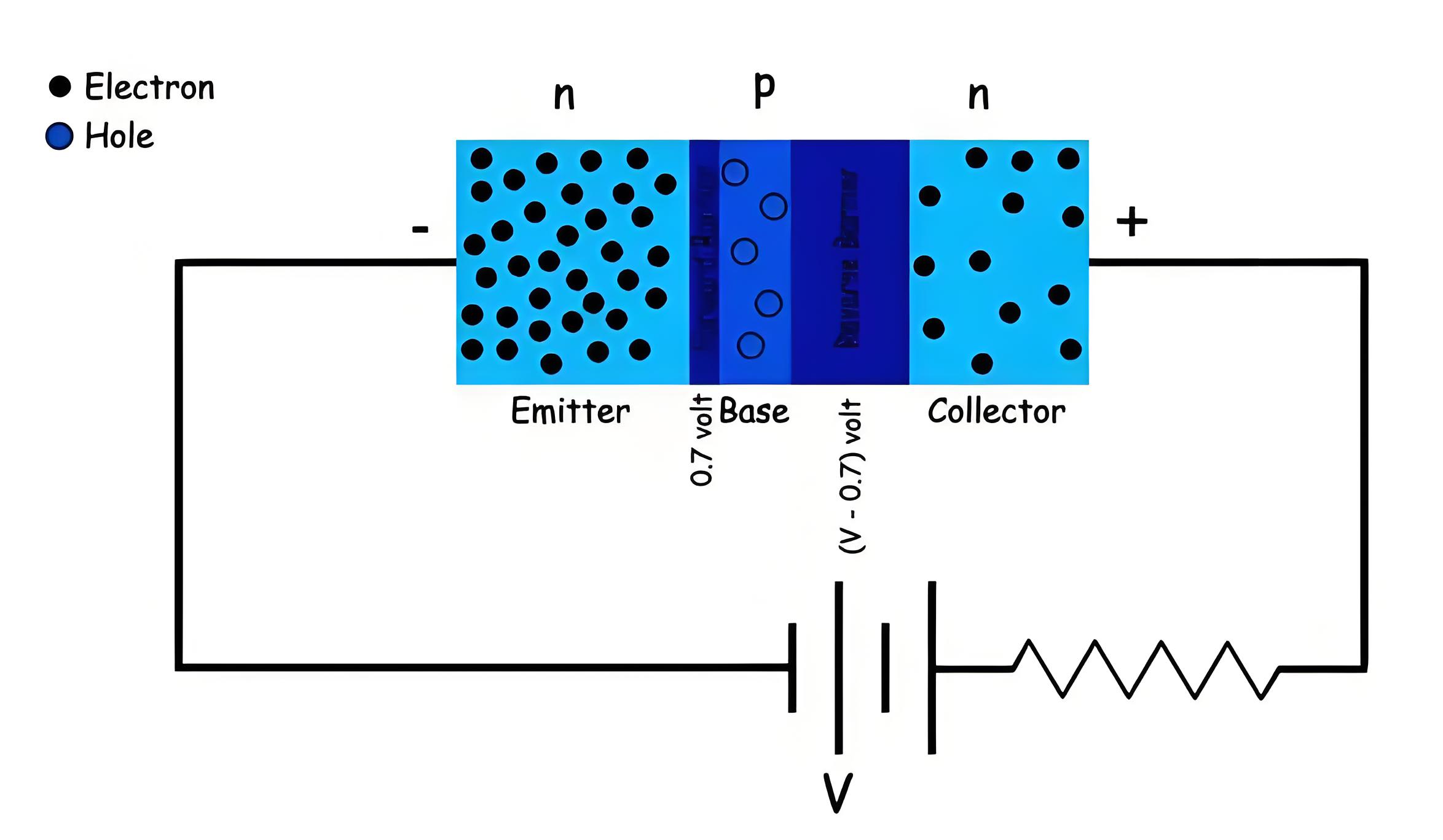
The base region, on the other hand, is very thin it is in the range of few micrometers whereas emitter and collector region are in the range of millimeter. The doping of the middle p-type layer is very low, and as a result, there is a very tiny number of holes present in this region. The collector region is wider as we already told and doping here is a moderate and hence moderate number of free electrons present in this region.
The voltage applied between the emitter and collector drops in two places. First, the emitter-base junction has a forward barrier potential of about 0.7 volts in silicon transistors. The rest of the voltage drops across the base-collector junction as a reverse barrier.
Whatever may be the voltage across the device the forward barrier potential across emitter-base junction always remains 0.7 volts and the rest of the source voltage is dropped across the base-collector junction as reverse barrier potential.
This means the collector voltage can’t overcome the forward barrier potential. So, the free electrons in the emitter can’t cross into the base. As a result, the transistor behaves like an off switch.
NB: – As at this condition the transistor does not conduct any current ideally, there will be no voltage drop at the external resistance hence entire source voltage (V) will drop across the junctions as shown in the figure above.
Now let us see what happens if we apply a positive voltage at the base terminal of the device. In this situation, the base-emitter junction gets forward voltage individually and certainly, it can overcome the forward potential barrier and hence the majority carriers, i.e., free electrons in the emitter region will cross the junction and come in the base region where they get very few numbers of holes to recombine.
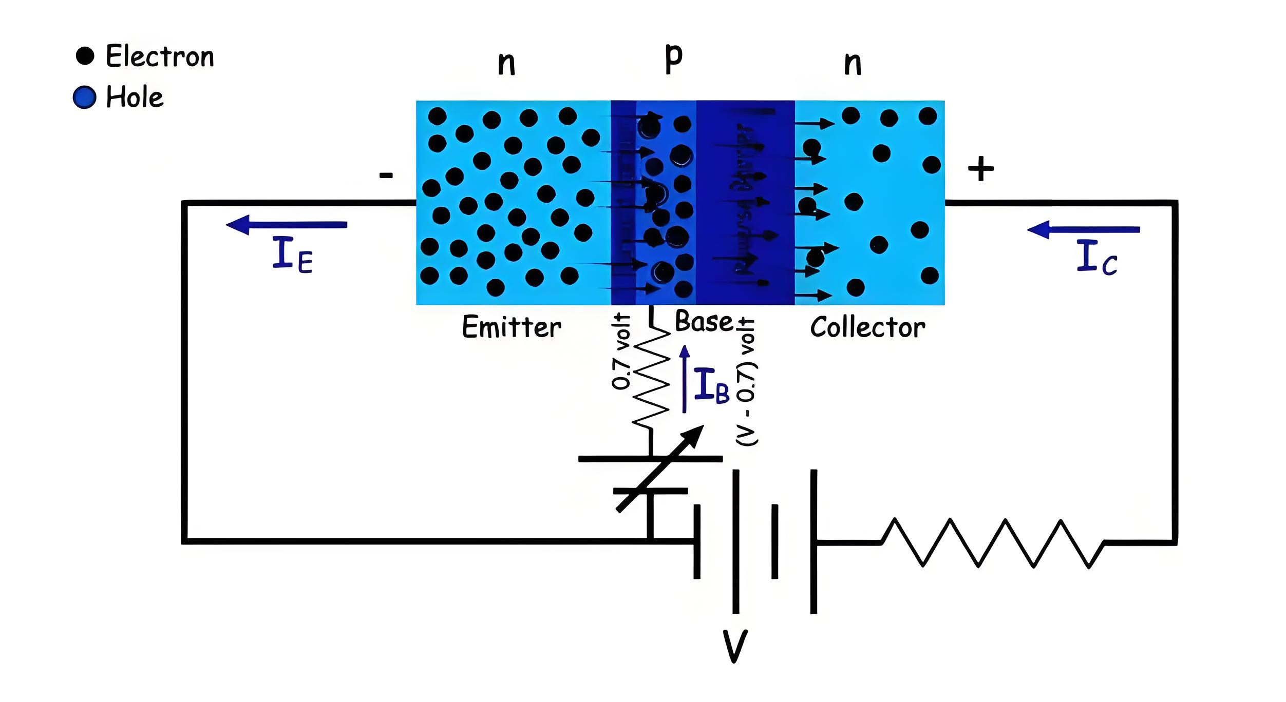
But due to the electric field across the junction, the free electrons migrating from emitter region get kinetic energy. The base region is so thin that the free electrons coming from emitter do not get sufficient time to recombine and hence cross the reverse biased depletion region and ultimately come to the collector zone. As there is a reverse barrier present across the base-collector junction, it will not obstruct the flow of free electrons from the base to the collector as the free electrons in the base region are minority carriers.
In this way, electrons flow from emitter to collector and hence collector to emitter current starts flowing. As there are few holes present in the base region some of the electrons coming from emitter region will recombine with these holes and contribute base current. This base current is quite smaller than collector to emitter current.
Some electrons from the emitter contribute to the base current, while most go through the collector. The emitter current is the total of the base and collector currents. So, the emitter current is the sum of the base and collector currents.
Now let us increase the applied base voltage. In this situation due to the increased forward voltage across emitter-base junction proportionately more free electrons will come from the emitter region to the base region with more kinetic energy. This causes a proportionate increase of collector current. In this way, by controlling a small base signal, we can control quite a large collector signal. This is the basic working principle of a transistor.
The Electricity Encyclopedia is dedicated to accelerating the dissemination and application of electricity knowledge and adding impetus to the development and innovation of the electricity industry.
