What are Transistor Characteristics ?
What are Transistor Characteristics ?
Transistor Characteristics define the relationship between the current and voltages in various transistor configurations. These configurations, similar to two-port networks, are analyzed through characteristic curves, categorized as follows:
Input Characteristics: These describe the changes in input current with the variation in the values of input voltage keeping the output voltage constant.
Output Characteristics: This is a plot of output current versus output voltage with constant input current.
Current Transfer Characteristics: This characteristic curve shows the variation of output current in accordance with the input current, keeping output voltage constant.
Common Base (CB) Configuration of Transistor
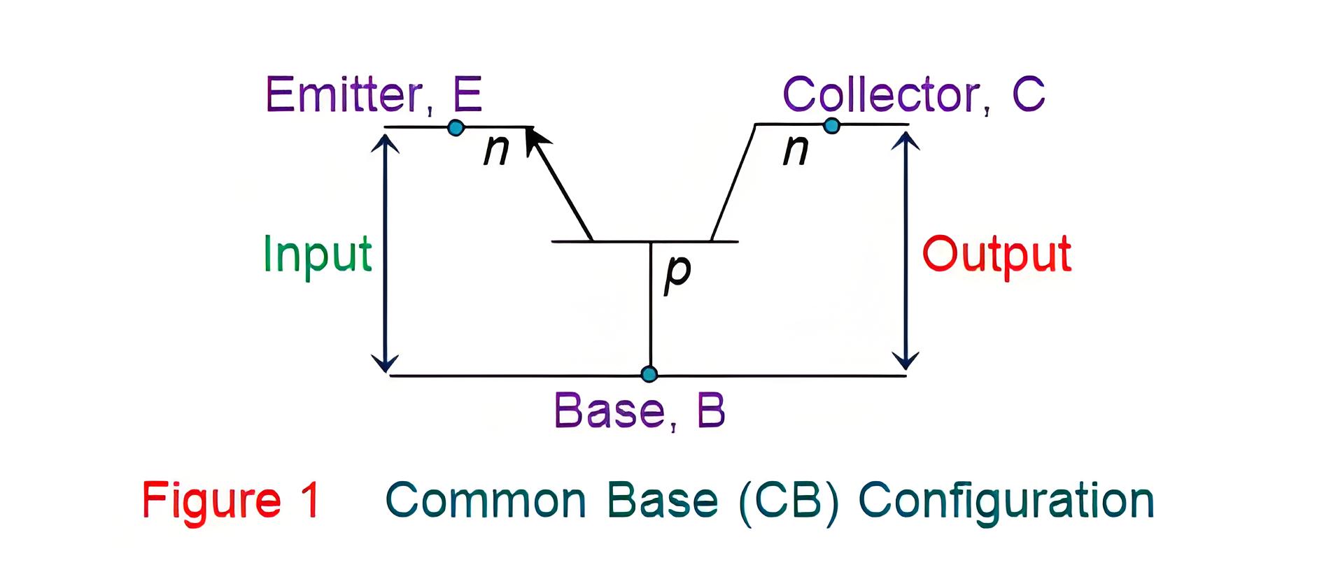
In CB Configuration, the base terminal of the transistor will be common between the input and the output terminals as shown by Figure 1. This configuration offers low input impedance, high output impedance, high resistance gain and high voltage gain.
Input Characteristics for CB Configuration of Transistor
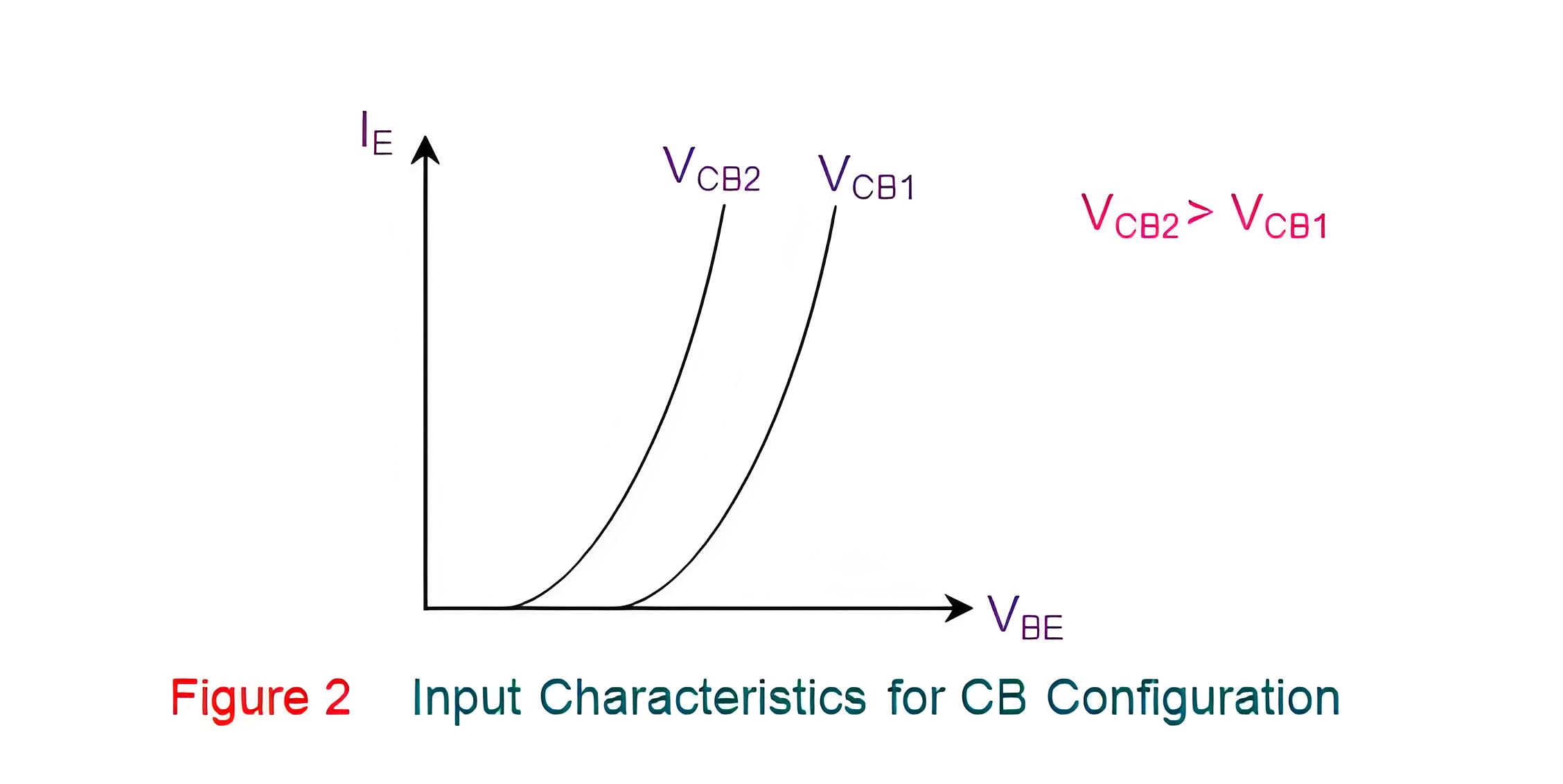
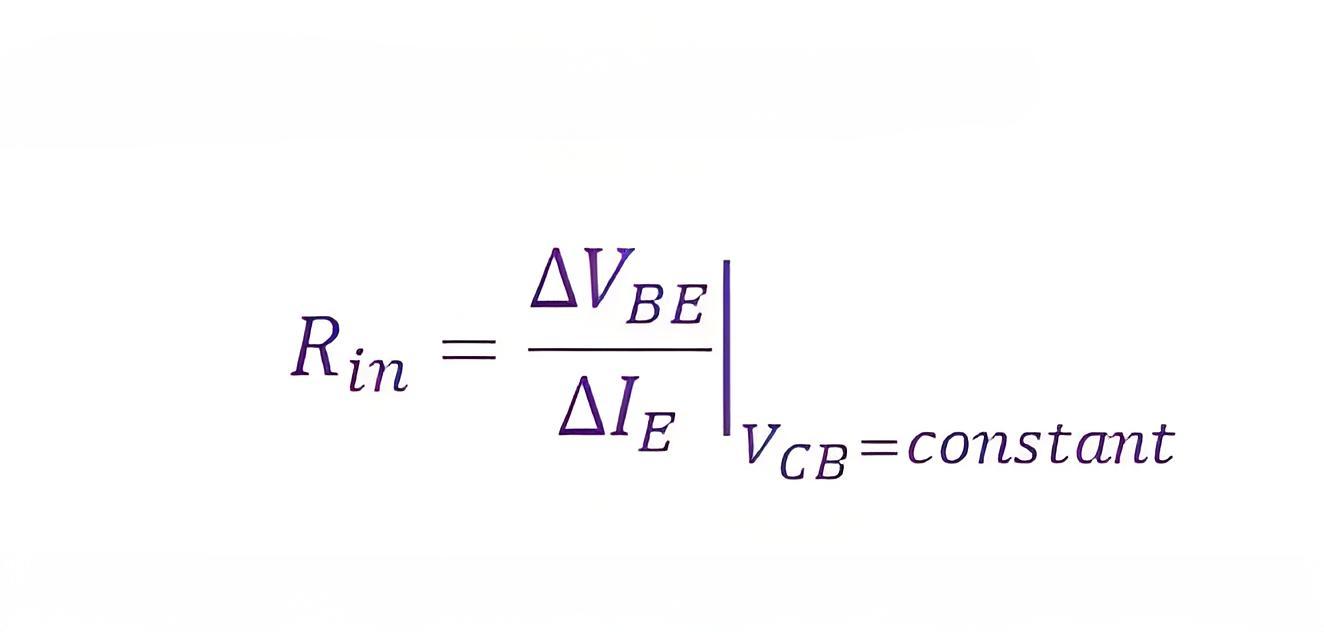
Input Characteristics for CB Configuration: Figure 2 illustrates how the emitter current, IE, varies with the Base-Emitter voltage, VBE, while keeping the Collector-Base voltage, VCB, constant.
This leads to the expression for the input resistance as
Output Characteristics for CB Configuration of Transistor
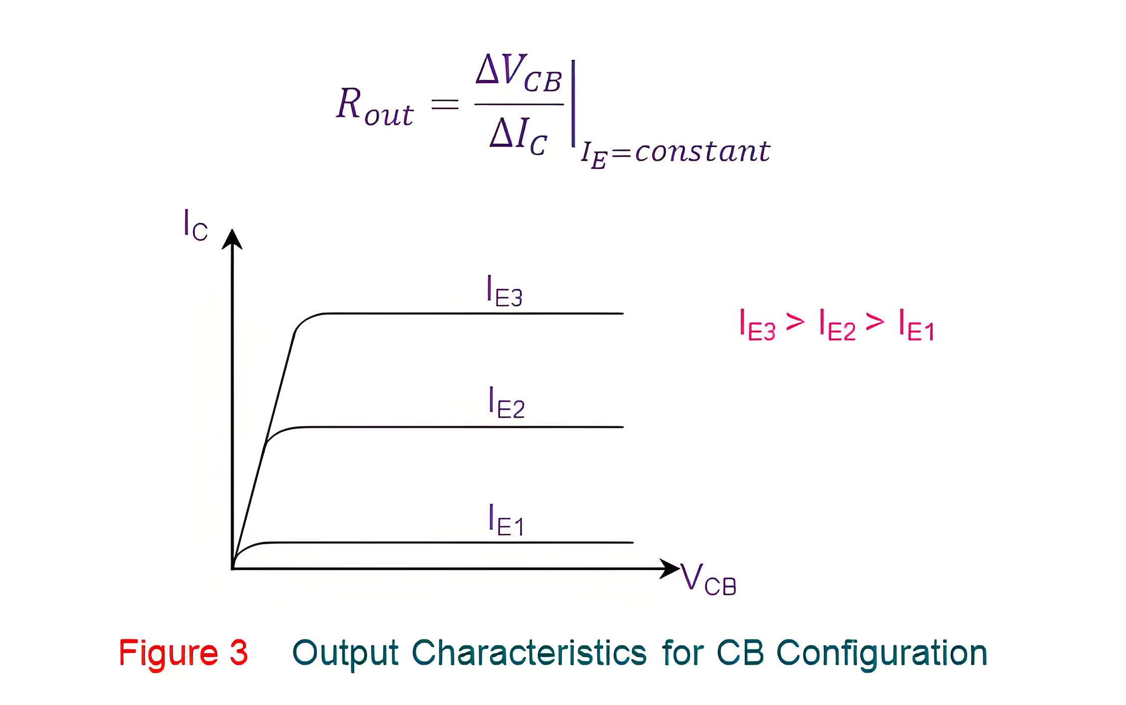
Output Characteristics for CB Configuration: Figure 3 displays the changes in collector current, IC, relative to VCB, maintaining a constant emitter current, IE. This graph also allows us to calculate the output resistance.
Current Transfer Characteristics for CB Configuration of Transistor
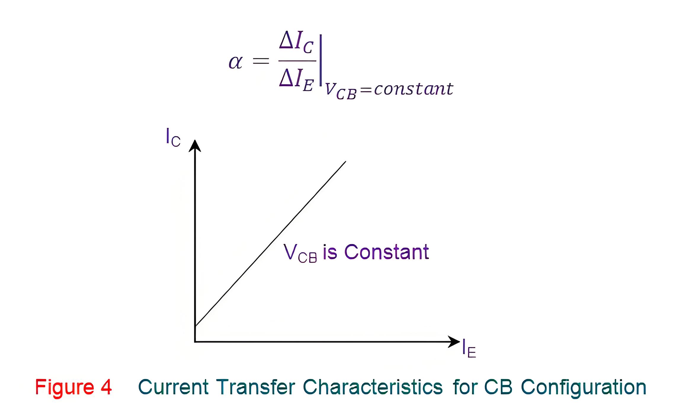
Current Transfer Characteristics for CB Configuration: Figure 4 presents how the collector current, IC, varies with the emitter current, IE, while keeping VCB constant. This results in a current gain of less than 1, expressed mathematically below.
Common Collector (CC) Configuration of Transistor
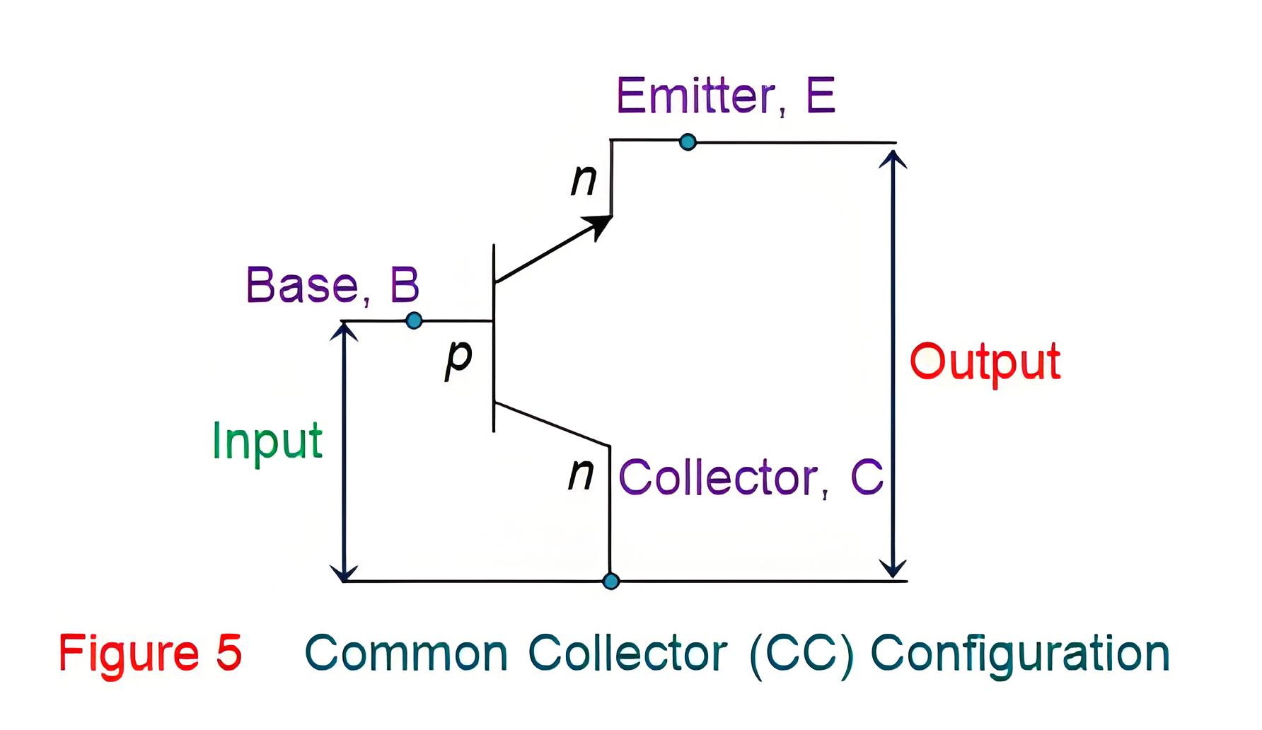
This transistor configuration has the collector terminal of the transistor common between the input and the output terminals (Figure 5) and is also referred to as emitter follower configuration. This offers high input impedance, low output impedance, voltage gain less than one and a large current gain.
Input Characteristics for CC Configuration of Transistor
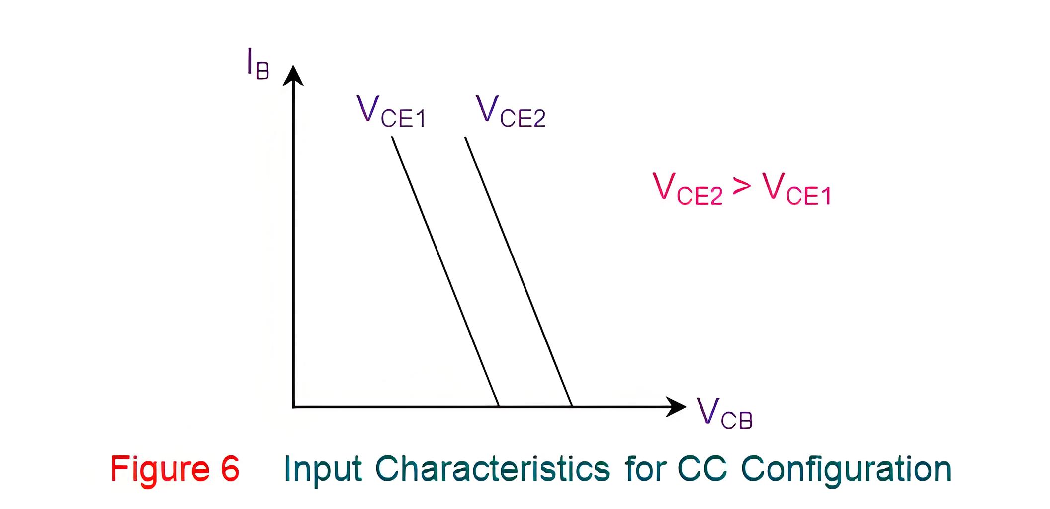
Input Characteristics for CC Configuration: Figure 6 outlines how the base current, IB, changes in relation to the Collector-Base voltage, VCB, with a constant Collector-Emitter voltage, VCE.
Output Characteristics for CC Configuration of Transistor
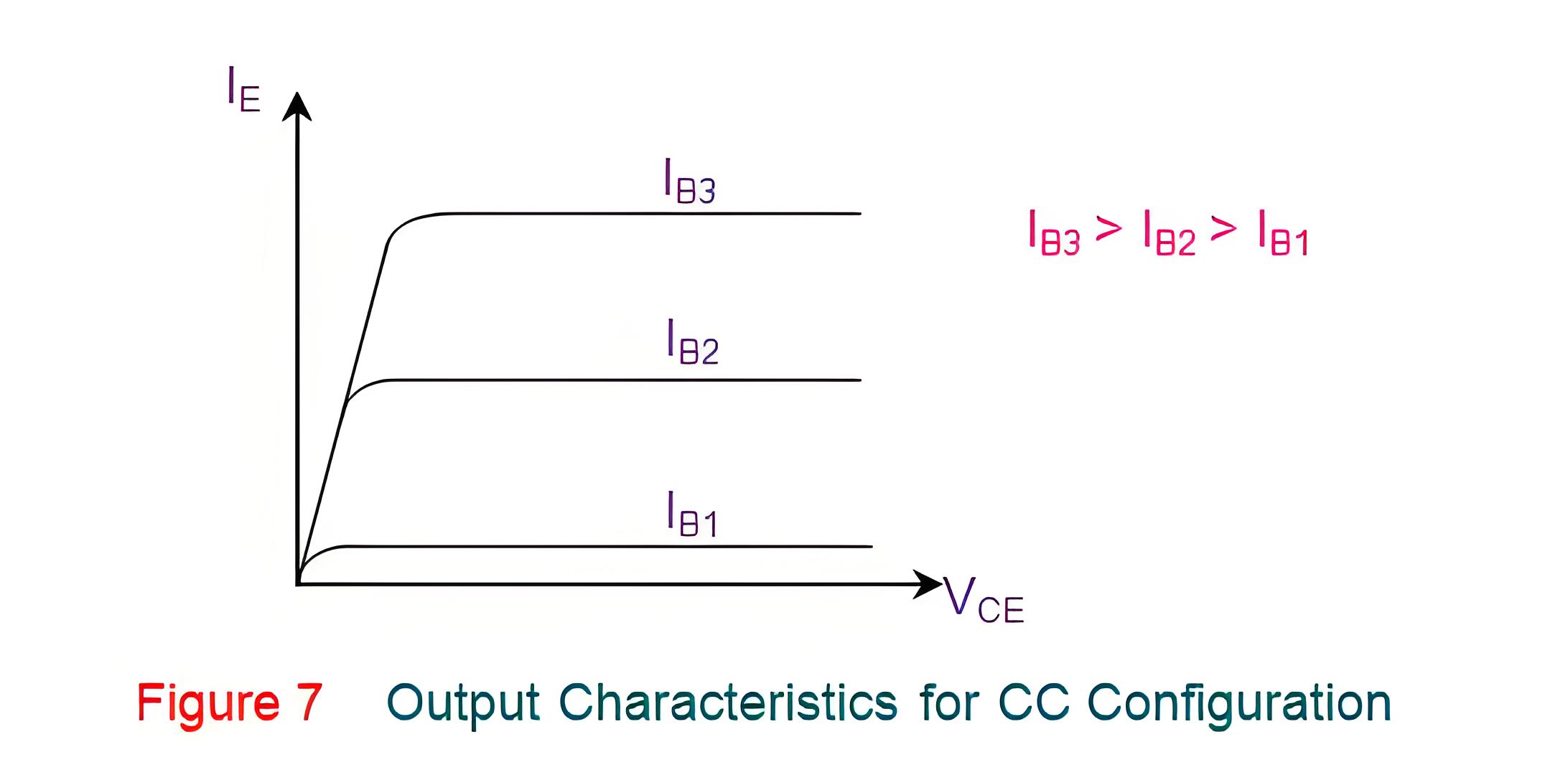
Figure 7 below shows the output characteristics for the CC configuration which exhibit the variations in IE against the changes in VCE for constant values of IB.
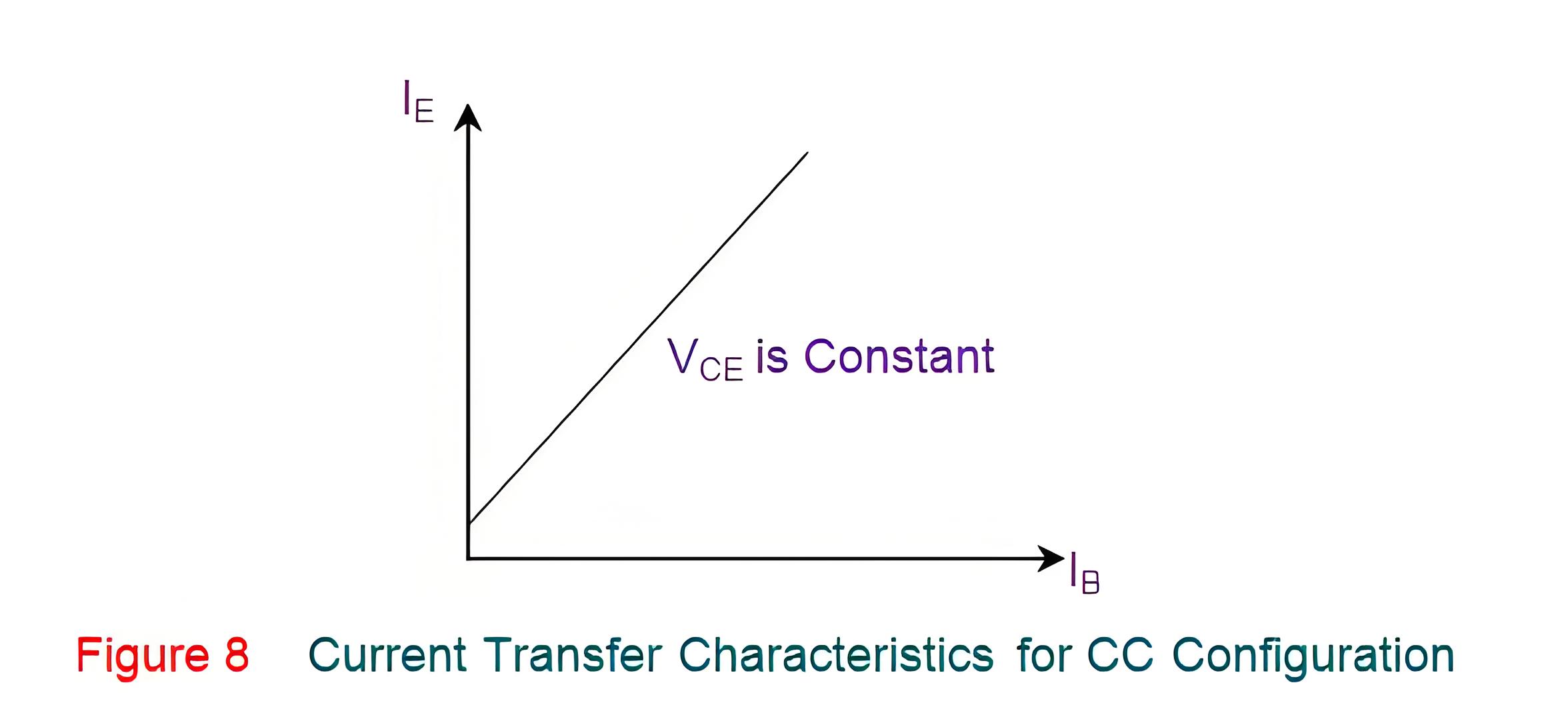
Current Transfer Characteristics for CC Configuration of Transistor
This characteristic of CC configuration (Figure 8) shows the variation of IE with IB keeping VCE as a constant.
Common Emitter (CE) Configuration of Transistor
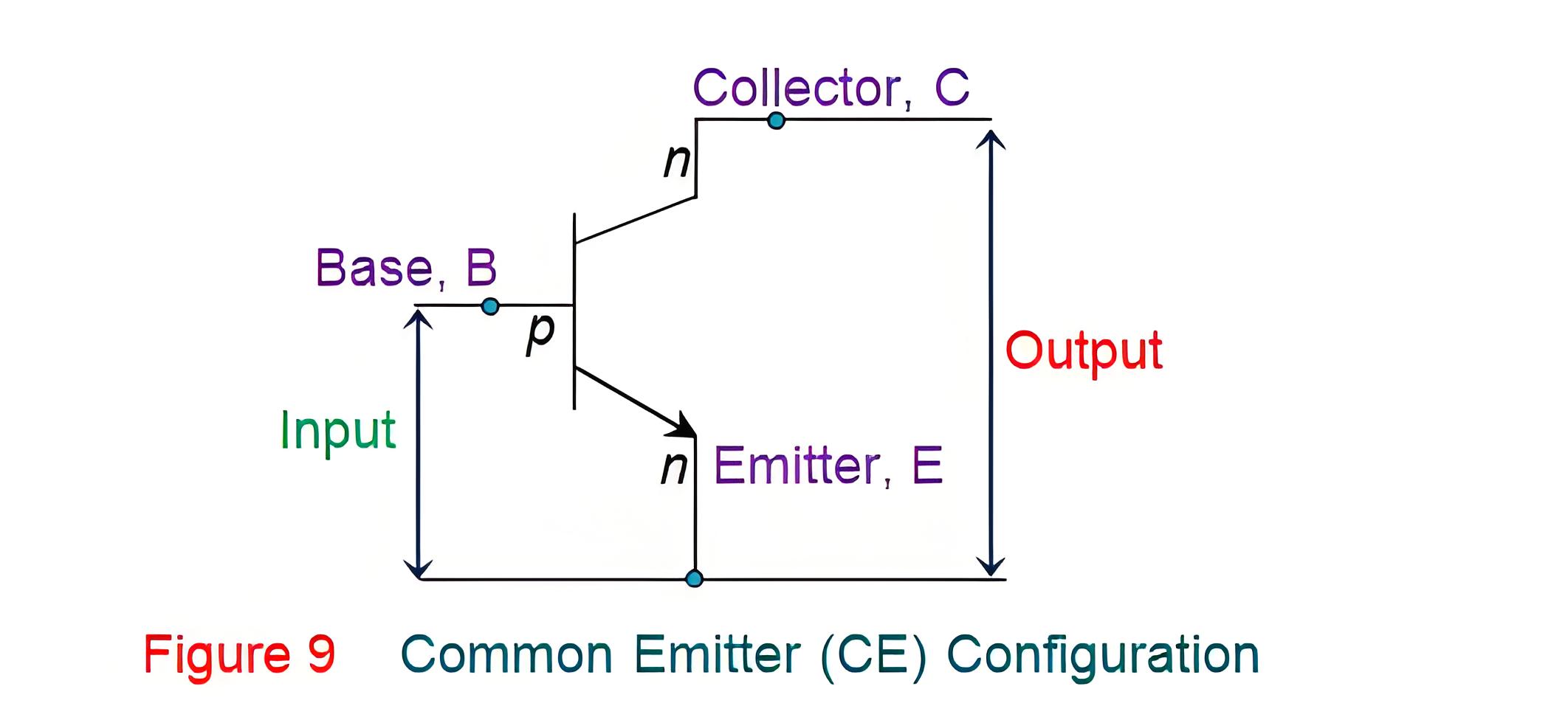
In this configuration, the emitter terminal is common between the input and the output terminals as shown by Figure 9. This configuration offers medium input impedance, medium output impedance, medium current gain and voltage gain.
Input Characteristics for CE Configuration of Transistor
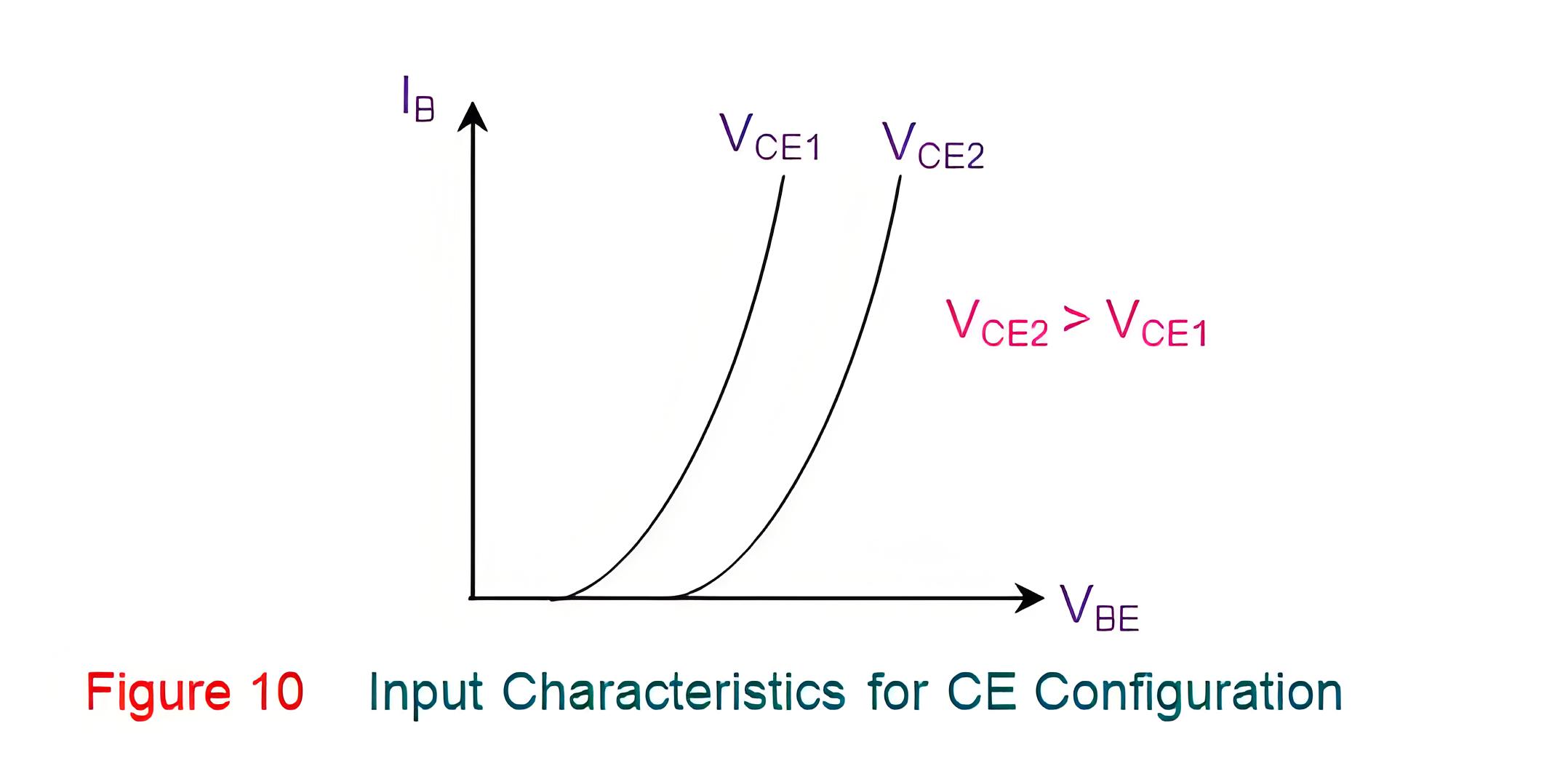
Figure 10 shows the input characteristics for the CE configuration of transistor which illustrates the variation in IB in accordance with VBE when VCE is kept constant.
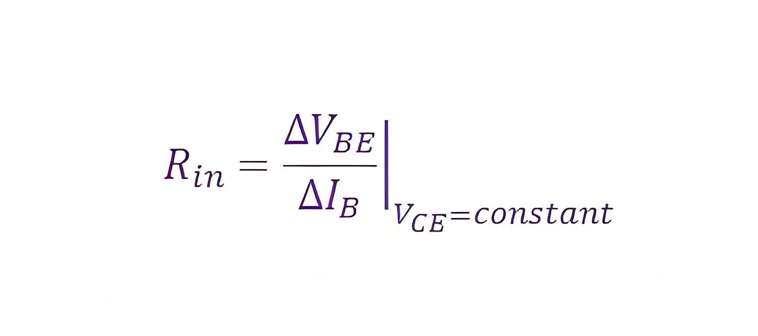
From the graph shown in Figure 10 above, the input resistance of the transistor can be obtained as
Output Characteristics for CE Configuration of Transistor
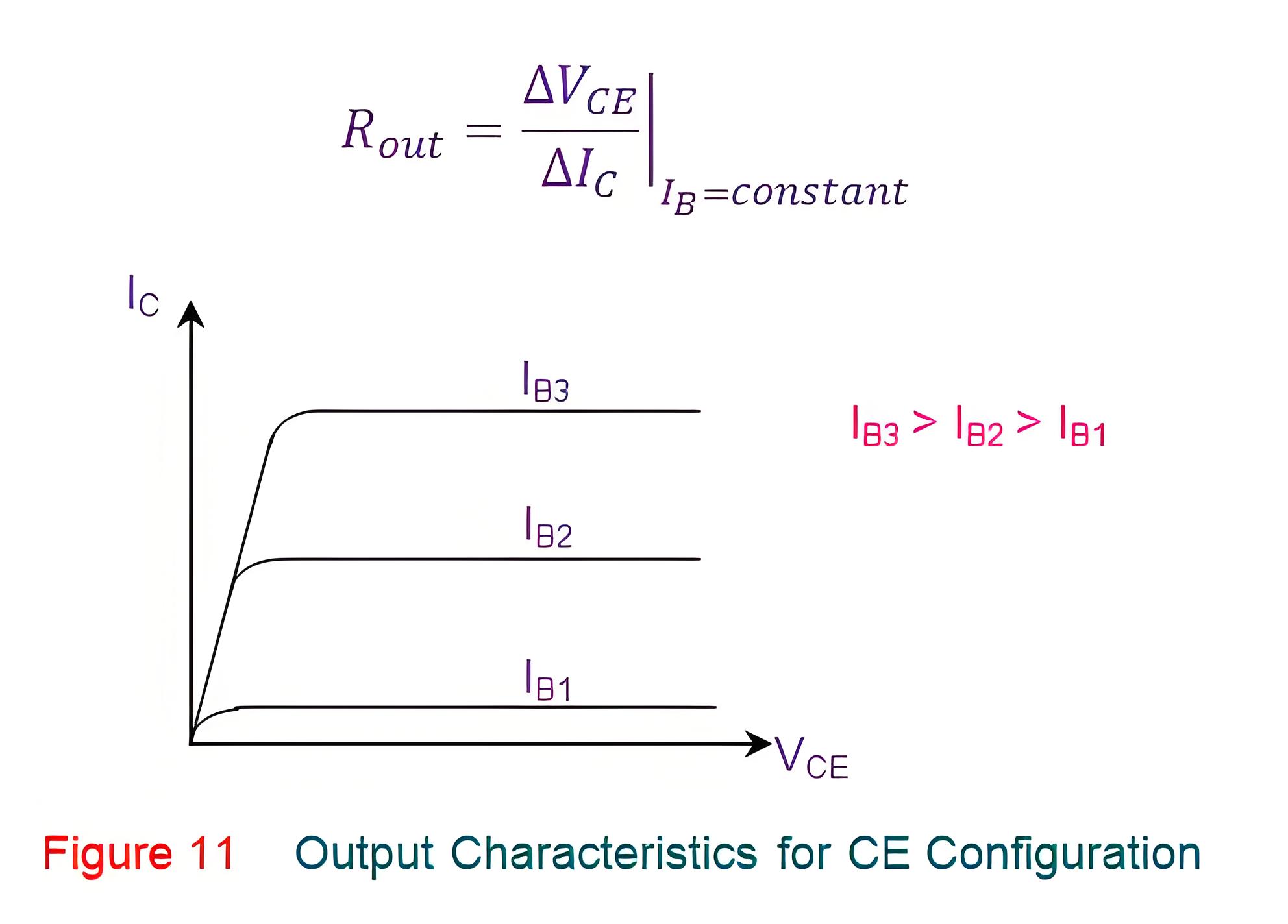
The output characteristics of CE configuration (Figure 11) are also referred to as collector characteristics. This plot shows the variation in IC with the changes in VCE when IB is held constant. From the graph shown, the output resistance can be obtained as:
Current Transfer Characteristics for CE Configuration of Transistor
This characteristic of CE configuration shows the variation of IC with IB keeping VCE as a constant. This can be mathematically given by

This ratio is referred to as common-emitter current gain and is always greater than 1.
Lastly, it is to be noted that although the characteristic curves explained are for BJTs, similar analysis holds good even in the case of FETs.
The Electricity Encyclopedia is dedicated to accelerating the dissemination and application of electricity knowledge and adding impetus to the development and innovation of the electricity industry.


