Transistor as an Amplifier
Transistor Definition
A transistor is defined as a semiconductor device with three terminals (Emitter, Base, and Collector) and two junctions (Base-Emitter and Base-Collector).
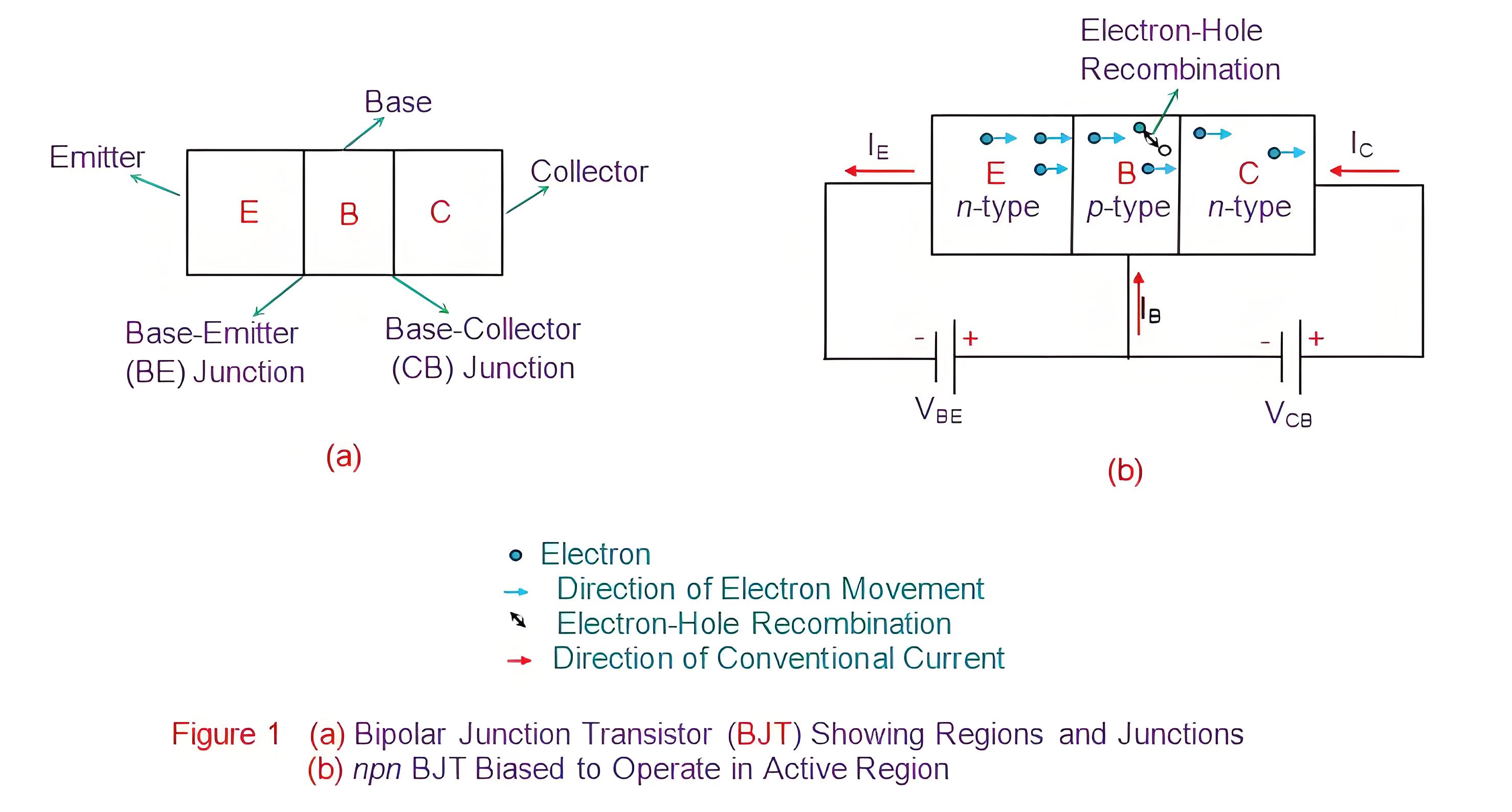
Transistor is a semiconductor device with three terminals: Emitter (E), Base (B), and Collector (C). It has two junctions: Base-Emitter (BE) and Base-Collector (BC). Transistors operate in three regions: cutoff (fully off), active (amplifying), and saturation (fully on).
When transistors operate in the active region, they act as amplifiers, increasing the strength of the input signal without significant alteration. This behavior is due to the movement of charge carriers. Consider an npn bipolar junction transistor (BJT) biased to operate in the active region, where the BE junction is forward biased and the BC junction is reverse biased.
In an npn transistor, the emitter is heavily doped, the base is lightly doped, and the collector is moderately doped. The base is narrow, while the emitter is broader, and the collector is the broadest.

The forward bias between the base and emitter terminals causes a small base current (IB) to flow into the base region. This current is usually in the microampere (μA) range, as VBE is typically around 0.6 V.
This process can be seen as electrons moving out of the base region or holes being injected into it. The injected holes attract electrons from the emitter, leading to the recombination of holes and electrons.
However due to the less doping of base in comparison with the emitter, there will be more number of electrons when compared to holes. Thus even after recombination effect, much more electrons will be left free. These electrons now cross the narrow base region and move towards the collector terminal influenced by the bias applied between the collector and the base regions.
This constitutes nothing but the collector current IC moving into the collector. From this it can be noticed that by varying the current flowing into the base region (IB), one can obtain a very large variation in collector current, IC. This is nothing but the current amplification, which leads to the conclusion that the npn transistor operating in its active region acts as a current amplifier. The associated current gain can be mathematically expressed as-

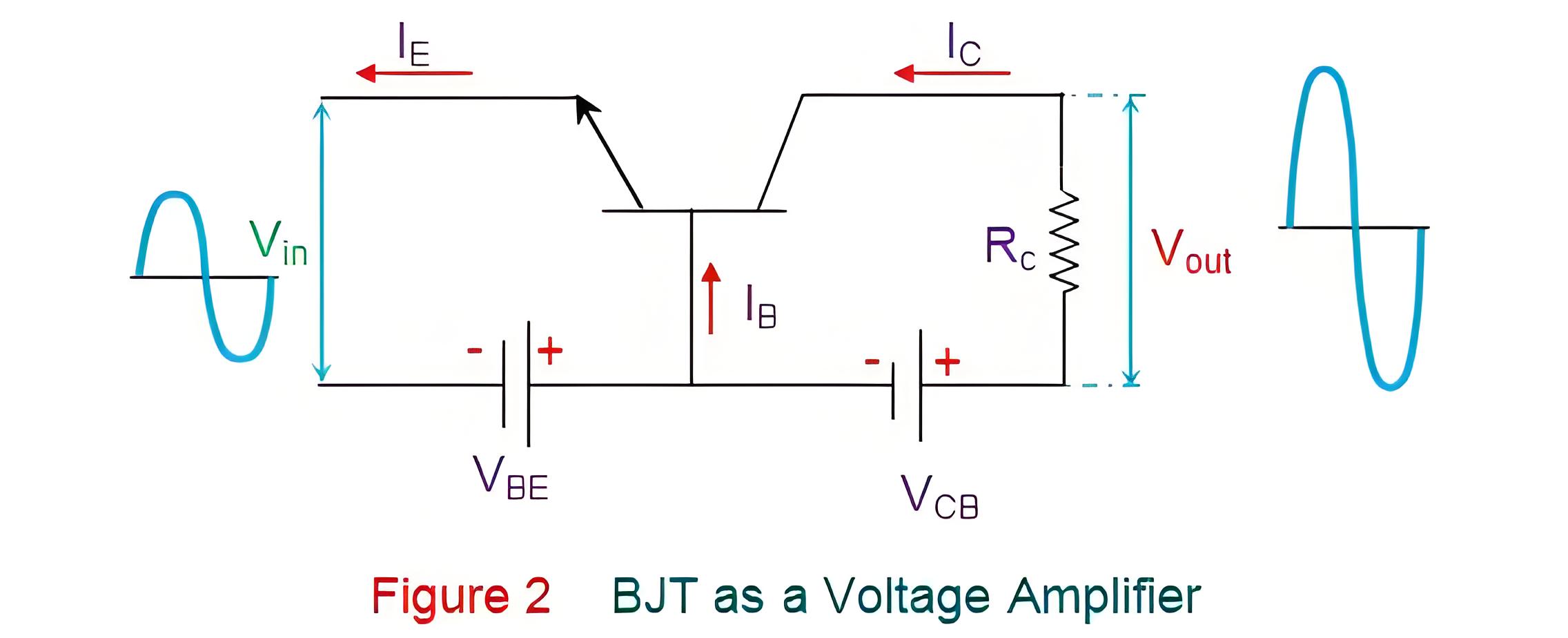
Now consider the npn transistor with the input signal applied between its base and emitter terminals, while the output being collected across the load resistor RC, connected across the collector and the base terminals, as shown by Figure 2.
Now consider the npn transistor with the input signal applied between its base and emitter terminals, while the output being collected across the load resistor RC, connected across the collector and the base terminals, as shown by Figure 2.
Further note that the transistor is always ensured to operate in its active region by using appropriate voltage supplies, V EE and VBC. Here a small change in the input voltage Vin is seen to change the emitter current IE appreciably as the resistance of the input circuit is low (due to the forward bias condition).

This in turn changes the collector current almost in the same range due to the fact that the magnitude of the base current is quite less for the case under consideration. This large change in IC causes a large voltage drop across the load resistor RC which is nothing but the output voltage.
Hence one gets the amplified version of the input voltage across the output terminals of the device which leads to the conclusion that the circuit acts like a voltage amplifier. Mathematical expression for the voltage gain associated with this phenomenon is given by
Although the explanation provided is for the npn BJT, similar analogy holds good for even pnp BJTs. Following on the same grounds, one can explain the amplifying action of other kind of transistor viz., Field Effect Transistor (FET). Further it is to be noted that there exist many variations to the amplifier circuit of transistors like

First Set: Common Base/Gate Configuration, Common Emitter/Source Configuration, Common Collector/Drain Configuration
Second Set: Class A amplifiers, Class B amplifiers, Class C Amplifiers, Class AB amplifiers
Third Set: Single Stage Amplifiers, Muti-Stage Amplifiers, and so on. However the basic working principle remains the same.
The Electricity Encyclopedia is dedicated to accelerating the dissemination and application of electricity knowledge and adding impetus to the development and innovation of the electricity industry.


