What is an PN Junction Diode?
What is an PN Junction Diode?
PN Junction Diode
A PN junction diode is a basic component in electronics. In this type of diode, one side of a semiconductor is doped with acceptor impurities (P-type) and the other side with donor impurities (N-type). This diode can be classified as either a ‘step graded’ or ‘linearly graded’ junction.
In a step graded PN junction diode, the dopant concentration is uniform on both sides up to the junction. In a linearly graded junction, the doping concentration changes almost linearly with the distance from the junction. Without any voltage applied, free electrons move to the P-side and holes move to the N-side, where they combine.
The acceptor atoms near the junction in the P-side become negative ions, and the donor atoms near the junction in the N-side become positive ions. This creates an electric field that opposes the further diffusion of electrons and holes. This region with uncovered ions is called the depletion region.
If, we apply forward bias voltage to the p-n junction diode. That means if the positive side of the battery is connected to the p-side, then the depletion regions width decreases and carriers (holes and free electrons) flow across the junction. If we apply a reverse bias voltage to the diode, the depletion width increases and no charge can flow across the junction.
P-N Junction Diode Characteristics
Let us consider a pn junction with a donor concentration ND and acceptor concentration NA. Let us also assume that all the donor atoms have donated free electrons and become positive donor ions and all the acceptor atoms have accepted electrons and created corresponding holes and become negative acceptor ions. So we can say the concentration of free electrons (n) and donor ions ND are the same and similarly, the concentration of holes (p) and acceptor ions (NA) are the same. Here, we have ignored the holes and free electrons created in the semiconductors due to unintentional impurities and defects.
Across the pn junction, the free electrons donated by donor atoms in n-type side diffuse to the p-typer side and recombine with holes. Similarly, the holes created by acceptor atoms in p-type side diffuse to the n-type side and recombine with free electrons. After this recombination process, there is a lack of or depletion of charge carriers (free electrons and holes) across the junction. The region across the junction where the free charge carriers get depleted is called depletion region.
Due to the absence of free charge carriers (free electrons and holes), the donor ions of n-type side and acceptor ions of p-type side across the junction become uncovered. These positive uncovered donor ions towards n-type side adjacent to the junction and negative uncovered acceptors ions towards p-type side adjacent to the junction cause a space charge across the pn junction. The potential developed across the junction due to this space charge is called the diffusion voltage. The diffusion voltage across a pn junction diode can be expressed as The diffusion potential creates a potential barrier for further migration of free electrons from n-type side to p-type side and holes from p-type side to n-type side. That means diffusion potential prevents charge carriers to cross the junction.
This region is highly resistive because of depletion of free charge carriers in this region. The width of the depletion region depends on the applied bias voltage. The relation between the width of the depletion region and bias voltage can be represented by an equation called Poisson Equation. Here, ε is the permittivity of the semiconductor and V is the biasing voltage. So, on an application of a forward bias voltage the width of the depletion region i.e. pn junction barrier decreases and ultimately disappears.
Hence, in absence of potential barrier across the junction in the forward bias condition free electrons enter into the p-type region and holes enter into the n-type region, where they recombine and release a photon at each recombination. As a result, there will be a forward current flowing through the diode. The current through the PN junction is expressed as Here, voltage V is applied across the pn junction and total current I, flows through the pn junction.
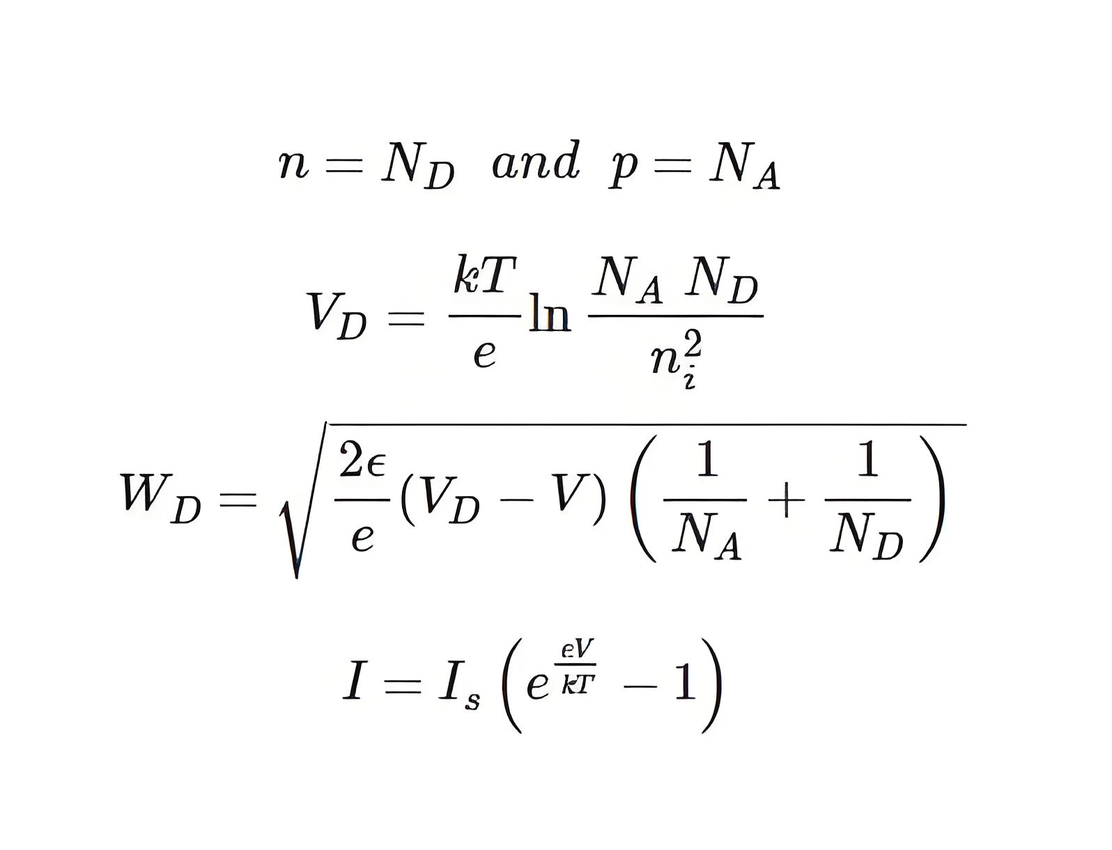
I s is reverse saturation current, e = charge of electron, k is Boltzmann constant and T is temperature in Kelvin scale.
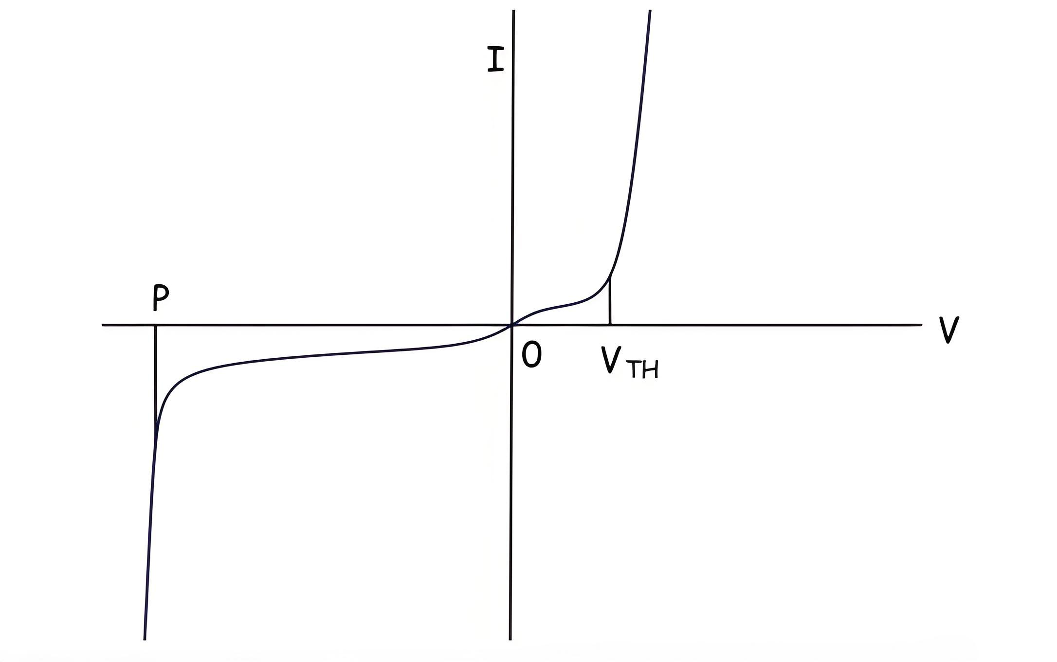
The graph below shows the current-voltage characteristic of a PN junction diode.When, V is positive the junction is forward biased, and when V is negative, the junction is reverse biased. When V is negative and less than VTH, the current is minimal. But when V exceeds VTH, the current suddenly becomes very high. The voltage VTH is known as the threshold or cut in voltage. For Silicon diode VTH = 0.6 V. At a reverse voltage corresponding to the point P, there is abrupt increment in reverse current. This portion of the characteristics is known as breakdown region.
Step Graded Junction
In a step graded junction, the concentration of dopants is uniform up to the junction on both sides.
Depletion Region
The depletion region forms at the junction where free electrons and holes recombine, creating an area with no free charge carriers.
Forward Bias
Applying a forward bias decreases the depletion region’s width, allowing current to flow.
Reverse Bias
Applying a reverse bias increases the depletion region’s width, blocking current flow until breakdown voltage is reached.
The Electricity Encyclopedia is dedicated to accelerating the dissemination and application of electricity knowledge and adding impetus to the development and innovation of the electricity industry.
