What is a PN Junction?
What is a PN Junction?
PN Junction Definition
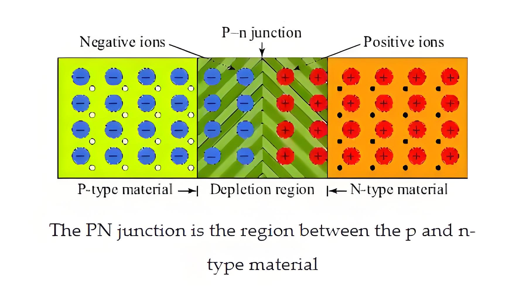
A PN junction is defined as an interface between p-type and n-type semiconductor materials in a single crystal.
Make a PN Junction
Let us now examine how this pn junction is created. There are plenty of holes in p-type semiconductor and plenty of free electrons in the n-type semiconductor.
Again in p-type semiconductor, there are numbers of trivalent impurity atoms, and ideally, each hole in the p-type semiconductor is associated with one trivalent impurity atom.
Here we use the word ‘ideal’ because we neglect thermally generated electrons and holes in the crystal. When an electron fills a hole, the impurity atom associated with that hole becomes a negative ion.
Because that now contains an extra electron. As the trivalent impurity atoms accept electrons and become negatively charged, the impurity is called acceptor impurity. The impurity atoms replace an equal number of semiconductor atoms in the crystal and place themselves in the crystal structure.
Hence, the impurity atoms are statics in the crystal structure. When these trivalent impurity atoms accept free electrons and become negative ions, the ions remain still static. Similarly, when a semiconductor crystal is doped with the pentavalent impurity, each atom of impurity replace semiconductor atom in the crystal structure; hence these impurity atoms become static in the crystal structure.
Each pentavalent impurity atom in the crystal structure has one extra electron in the outermost orbit which it can easily remove as a free electron. When it removes that electron it becomes positively charged ions.

Since pentavalent impurity atoms donate electrons to the semiconductor crystal, they are called donor impurities. We discuss static acceptor and donor impurity atoms because they play a key role in forming the PN junction.
Let us come to the point when a p-type semiconductor comes in contact with an n-type semiconductor, free electrons on n-type semiconductor nearer to the junction first migrate to the p-type semiconductor due to diffusion because the concentration of free electrons is much more in the n-type region than that of the p-type region.
The electrons come to the p region will combine with holes they first find. That means the free electrons come from the n-type region will combine with acceptor impurity atoms nearer to the junction. This phenomenon makes negative ions.
As the acceptor impurity atoms nearer the junction in the p-type region, become negative ions, there will be a layer of negative static ions in p region adjacent to the junction.
The free electrons in the n-type region will migrate first to the p-type region than the free electrons in the n-type region away from the junction. This makes a layer of static positive ions in the n-type region adjacent to the junction.
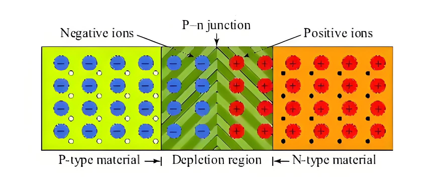
After the formation of the sufficiently thick positive ions layer in the n-type region and negative ions layer in the p-type region, there will be no more diffusion of electrons from n-type region to p-type region as because there is a negative wall in front of free electrons. These both layers of ions from the PN junction.
Since one layer is negatively charged and the other is positively charged, an electrical potential forms across the junction, acting as a potential barrier. This barrier potential depends on the semiconductor material, doping level, and temperature.
It is found that barrier potential for germanium semiconductor is 0.3 volt at 25oC, and it is for silicon semiconductor 0.7 volt at the same temperature.
This potential barrier does not contain any free electron or hole since all free electrons are combined with holes in this region and due to the depletion of charge carriers (electrons or holes) in this region, it is also called depletion region. Although diffusion of free electrons and holes stop after the creation of certain thick depletion layer practically this thickness of depletion layer is very tiny it in a range of micrometres.
The Electricity Encyclopedia is dedicated to accelerating the dissemination and application of electricity knowledge and adding impetus to the development and innovation of the electricity industry.
