What is a PIN Diode?
What is a PIN Diode?
PIN Diode Definition
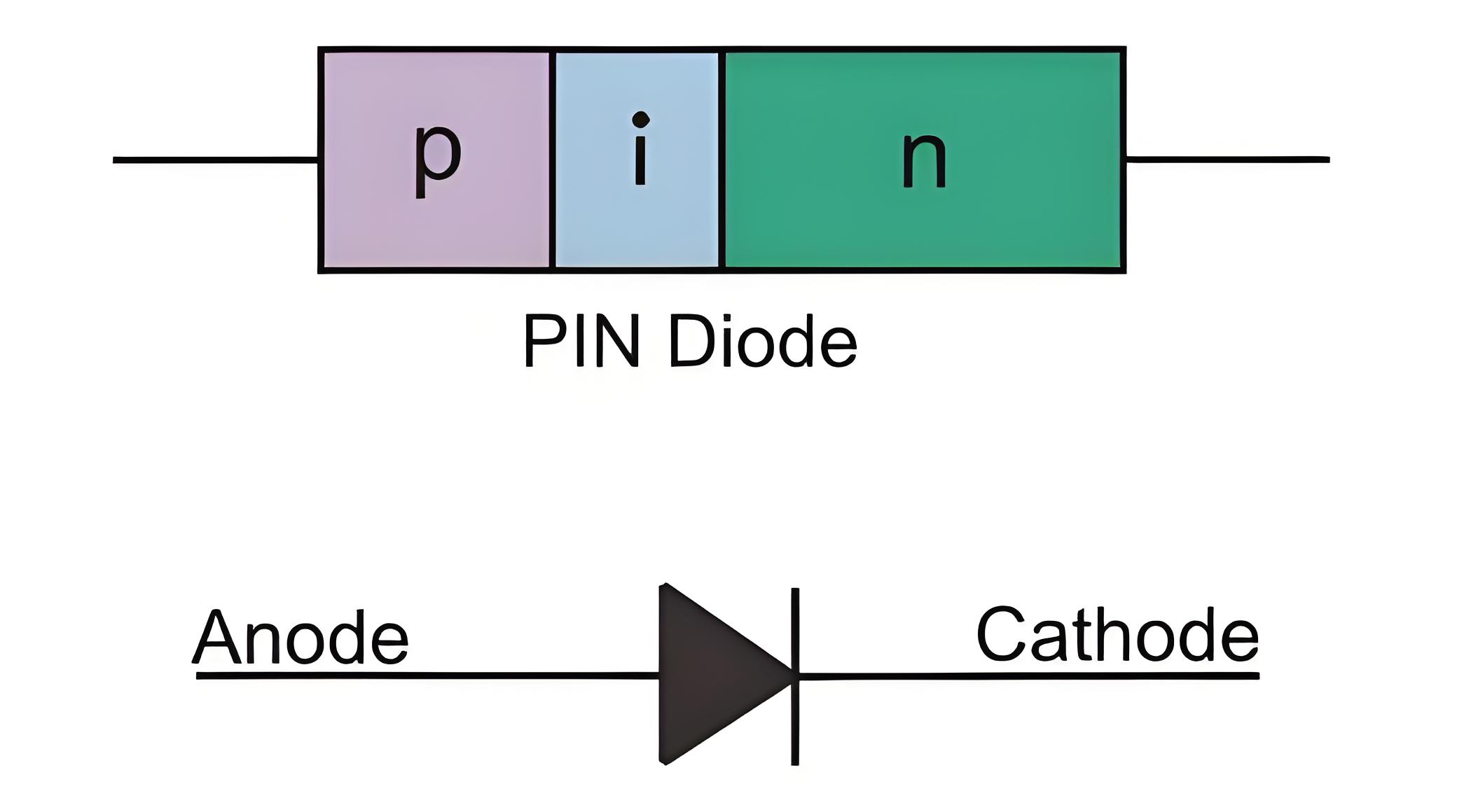
A PIN diode is a specific type of diode that features an undoped intrinsic semiconductor layer of silicon or germanium between the heavily doped p-type semiconductor and n-type semiconductor layers. Unlike standard diodes, it includes this additional layer, which poorly conducts electric current but is essential for certain electronic applications. It’s like having a p region, followed by an intrinsic region and then an N region, thus making it a PIN diode and hence derived the name from the same.
Symbol of PIN Diode

Construction of a PIN Diode
As already explained, a pin diode has an intrinsic undopedlayer (having high resistivity) sandwiched between a PN junction, we will now look at the construction of the diode in detail.
PIN diodes are constructed using either Mesa or Planar structures. In the Mesa structure, pre-doped layers are added to the substrate, allowing control over the doping level and layer thickness. The Planar structure involves growing an epitaxial layer on the substrate, with the p+ region formed by ion implantation or diffusion.
Working of the PIN Diode
Though similar to regular diodes in operation, PIN diodes include an extra intrinsic layer that makes them less effective as rectifiers but excellent for uses like switches and attenuators.
Forward biased operation of PIN Diode
In forward bias, the depletion region at the PIN diode’s p-n junction decreases, enabling current flow. This reduction allows the diode to act as a variable resistor and develop a high electric field that accelerates charge carriers, enhancing its performance in high-frequency applications.
Reverse biased operation of PIN Diode
When the pin diode is in reverse biased condition, the width of the depletion region increases. At a certain reverse bias voltage, the entire intrinsic layer will be swept out of charge carriers. This voltage is called the swept in voltage. The value is -2v. It is used for switching purposes while in reverse bias.
Characteristics of PIN Diode
At a lower level of reverse bias, the depletion layer becomes fully depleted. The capacitance of the pin diode becomes independent of the level of bias once the depletion layer is fully depleted. This is because there is very little net charge in the intrinsic layer. The leakage of RF signal is lower than other diodes because the level of capacitance is typically lower.
In forward bias, the diode behaves as a resistor than a non-linear device and produces no rectification or distortion. The value of the resistance depends on the bias voltage. Pin diode is used as RF switch or variable resistor as they produce fewer distortions than a normal diode.
Application of PIN Diode
RF switch
High Voltage Rectifier
Photodetector
The Electricity Encyclopedia is dedicated to accelerating the dissemination and application of electricity knowledge and adding impetus to the development and innovation of the electricity industry.


