What are Intrinsic Silicon and Extrinsic Silicon ?
What are Intrinsic Silicon and Extrinsic Silicon ?
Intrinsic Silicon
Silicon is a vital element semiconductor. Silicon is a group IV material. In its outer orbit, it has four valence electrons which held by covalent bonds with the valence electrons of four adjacent silicon atoms. These valence electrons are not available for electricity. So, at OoK intrinsic silicon behaves like an insulator. When the temperature rises, some valence electrons break their covalent bonds due to thermal energy. This creates a vacancy, known as a hole, where the electron was. In other words at any temperature greater that 0oK some of the valence electrons in the semiconductor crystal gain sufficient energy to jump to conduction band from valance band and leave behind a hole in the valence band. This energy is approximately equal to 1.2 eV in room temperature (i.e. at 300oK) which is equal to the band gap energy of silicon.
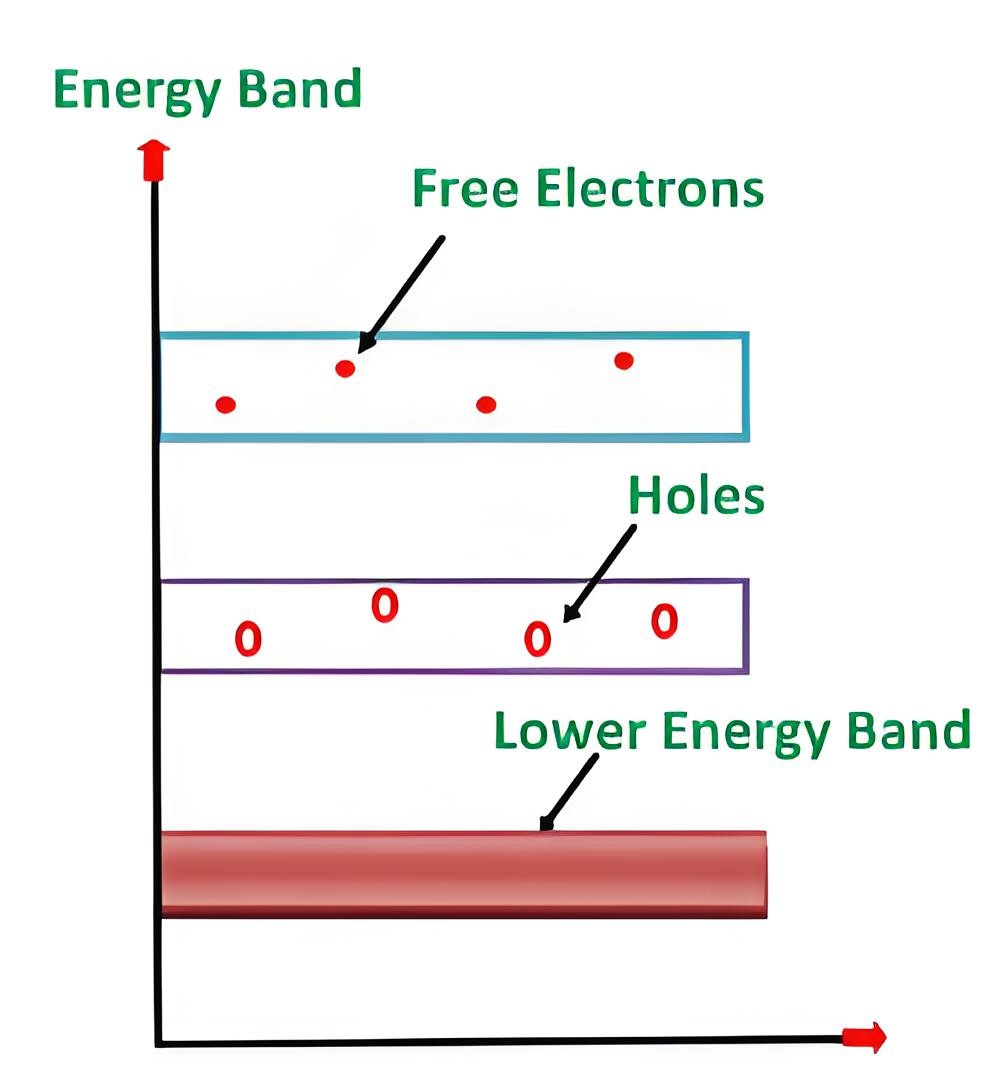
In the intrinsic silicon crystal, the number of holes is equal to the number of free electrons. Since each electron when leaves the covalent bond contributes a hole in the broken bond. At a certain temperature, new electron-hole pairs are continuously created by thermal energy, while an equal number of pairs recombine. Hence at a particular temperature in a certain volume of insintric silicon number of electron-hole pairs remain same. This is an equilibrium condition. Hence, this is obvious that in the equilibrium condition, the free electrons concentration n and the holes concentration p are equal to each other, and this is nothing but intrinsic charge carrier concentration(ni). i.e, n = p = ni. The atomic structure is shown below.
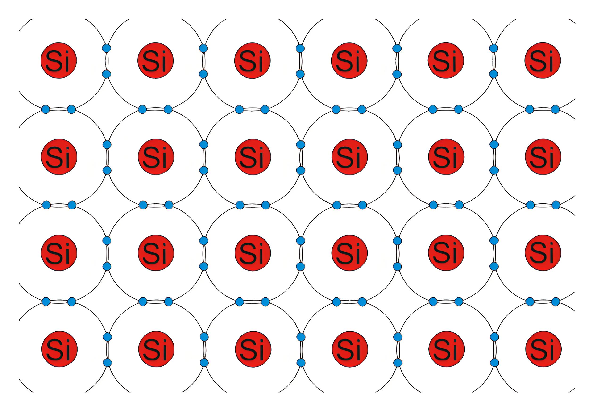
Intrinsic Silicon at 0oK
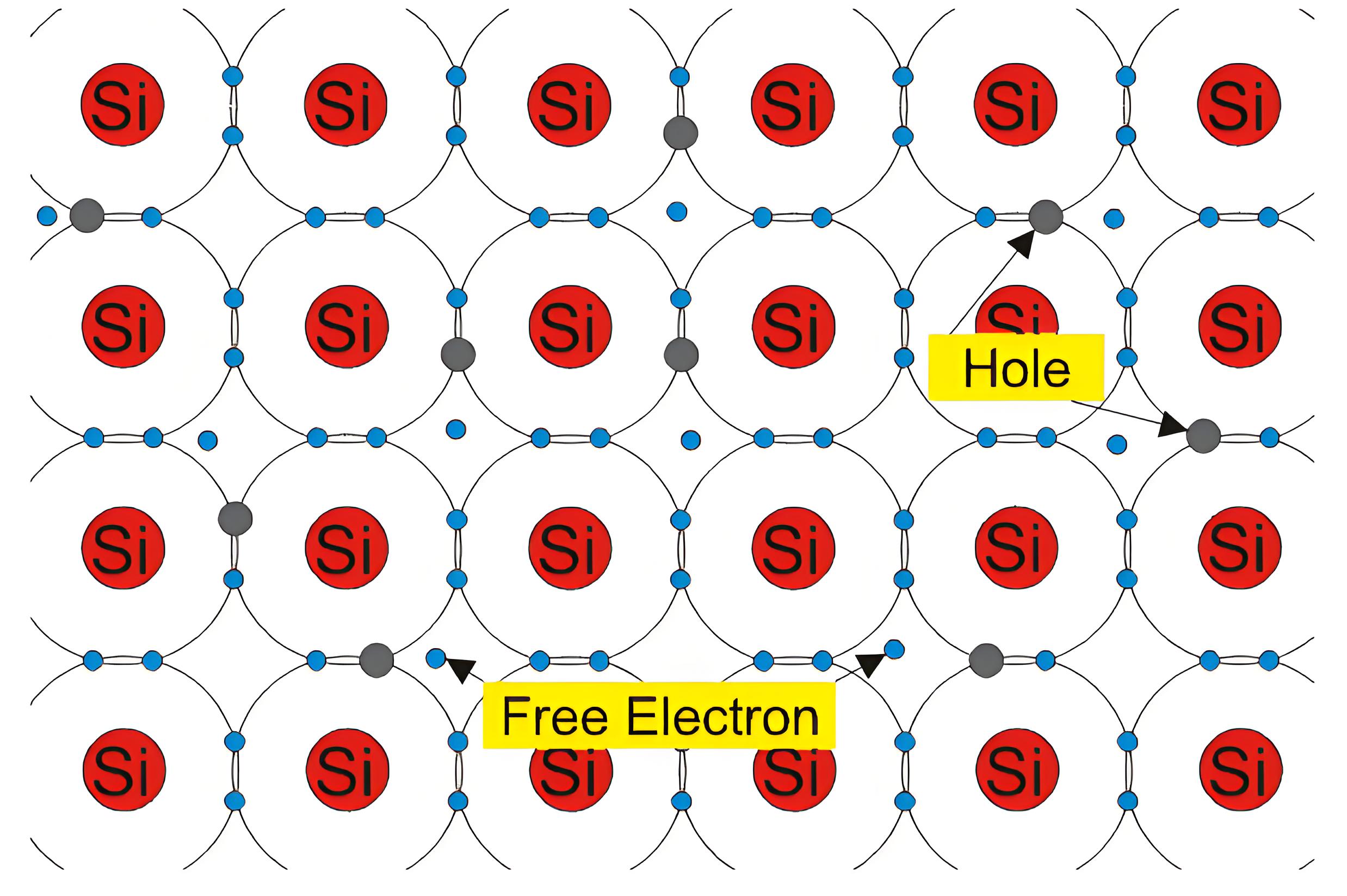
Intrinsic Silicon at Room Temperature
Extrinsic Silicon
Intrinsic silicon can be turned in to extrinsic silicon when it is doped with controlled amount of dopants. It is doped with donor atom (group V elements) it becomes n-type semiconductor and when it is doped with acceptor atoms (group III elements) it becomes p-type semiconductor.
Let a small amount of group V element is added to an intrinsic silicon crystal. The examples of group V elements are phosphorus (P), arsenic (As), antimony (Sb) and bismuth (Bi). They have five valence electrons. When they displace a Si atom, the four valence electrons make covalent bonds with neighboring atoms and the fifth electron which does not participate in forming the covalent bond is loosely attached to the parent atom and can easily leave the atom as a free electron. The energy necessary for silicon this purpose that is for releasing that fifth electron is about 0.05 eV. This kind of impurity is named as the donor as this contributes free electrons to the silicon crystal. The silicon is known as n- type or negative type silicon as the electrons are negatively charged particles.
The Fermi Energy Level moves closer to the conduction band in the n-type silicon. Here the number of free electrons is increased over intrinsic concentration of electrons. On the other hand, the number of holes is decreased over intrinsic hole concentration as there is more probability of recombination due to the larger number of free electrons concentration. Electrons are majority charge carriers.
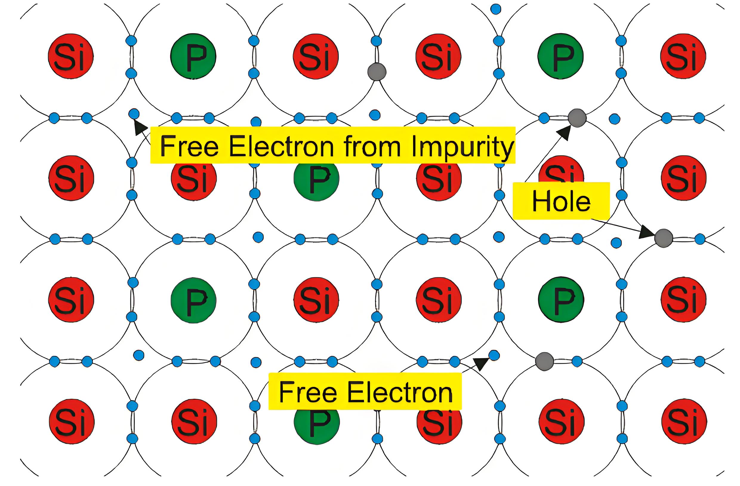
Extrinsic Silicon with Pentavalent Impurity
If a small amount of group III elements is added to an intrinsic semiconductor crystal, then they displace a silicon atom, group III elements like AI, B, IN have three valence electrons. These three electrons make the covalent bonds with neighboring atoms creating a hole. These kinds of impurity atoms known as acceptors. The semiconductor in known as p-type semiconductor as the hole is assumed to be positively charged.
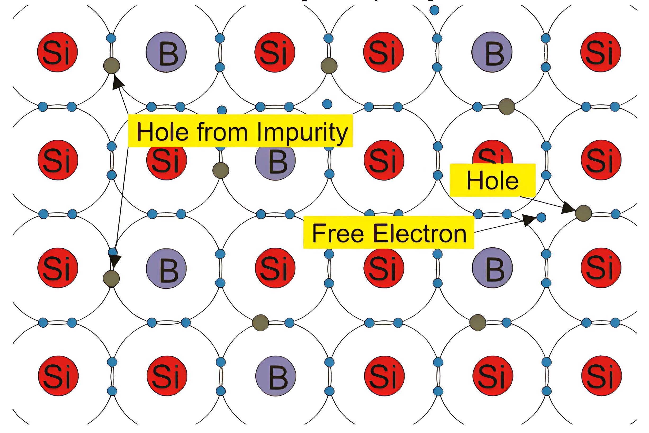
Extrinsic Silicon with Trivalent Impurity
The Fermi energy level in p-type semiconductors moves closer to the valence band. The number of holes increases, while the number of electrons decreases compared to intrinsic silicon. In p-type semiconductors, holes are the majority charge carriers.
Intrinsic Carrier Concentration of Silicon
When an electron jumps from valence band to conduction band because of thermal excitation, free carriers are created in both bands that are electron in the conduction band and hole in the valence band. The concentration of these carriers is known as intrinsic carrier concentration. Practically in pure or intrinsic silicon crystal the number of holes (p) and electrons (n) are equal to each other, and they are equal to intrinsic carrier concentration ni. Therefore, n = p = ni
The no. of these carriers depends on the band gap energy. For silicon, the band gap energy is 1.2 eV at 298oK intrinsic carrier concentration in silicon increases with the increase of temperature. Intrinsic carriers concentration in silicon is given by,
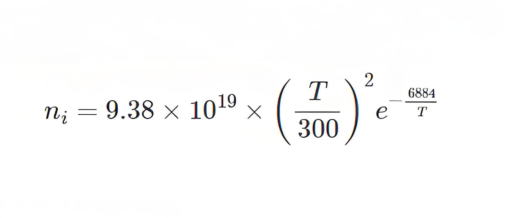
Here, T = temperature in absolute scale
The intrinsic carrier concentration at 300oK is 1.01 × 1010 cm-3. But the previously accepted value is 1.5 × 1010 cm-3.
The Electricity Encyclopedia is dedicated to accelerating the dissemination and application of electricity knowledge and adding impetus to the development and innovation of the electricity industry.


