Bipolar Junction Transistor
BJT Definition
A Bipolar Junction Transistor (also known as a BJT or BJT Transistor) is a three-terminal semiconductor device consisting of two p-n junctions which are able to amplify or magnify a signal. It is a current controlled device. The three terminals of the BJT are the base, the collector and the emitter. A BJT is a type of transistor that uses both electrons and holes as charge carriers.
A signal of small amplitude if applied to the base is available in the amplified form at the collector of the transistor. This is the amplification provided by the BJT. Note that it does require an external source of DC power supply to carry out the amplification process.
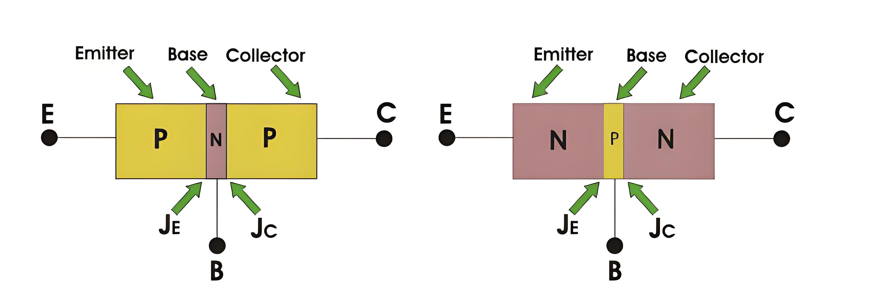
There are two types of bipolar junction transistors – NPN transistors and PNP transistors. A diagram of these two types of bipolar junction transistors is given below.
From the above figure, we can see that every BJT has three parts named emitter, base and collector. JE and JC represent the junction of emitter and junction of collector respectively. Now initially it is sufficient for us to know that emitter based junction is forward biased and collector-base junctions are reverse biased. The next topic will describe the two types of these transistors.
NPN Bipolar Junction Transistor
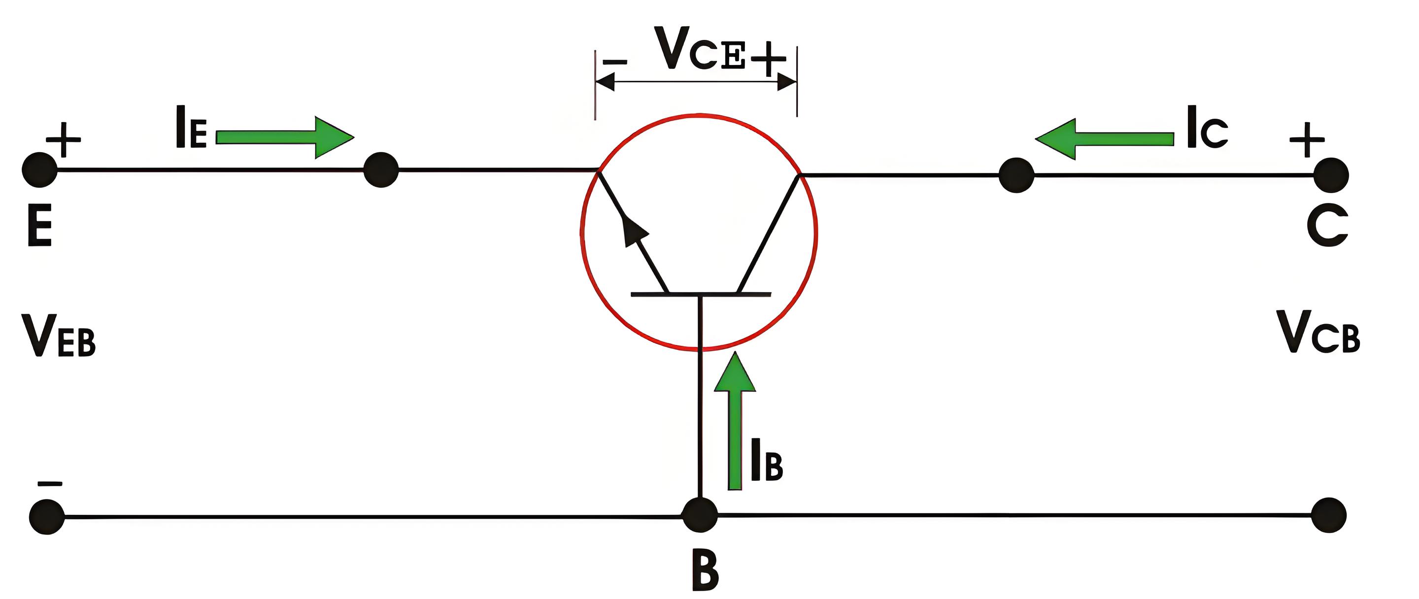
In an n-p-n bipolar transistor (or npn transistor) one p-type semiconductor resides between two n-type semiconductors the diagram below an n-p-n transistor is shown Now I E, IC is emitter current and collect current respectively and VEB and VCB are emitter-base voltage and collector-base voltage respectively. According to the convention if for the emitter, base and collector current IE, IB and IC current goes into the transistor the sign of the current is taken as positive and if current goes out from the transistor then the sign is taken as negative. We can tabulate the different currents and voltages inside the n-p-n transistor.
PNP Bipolar Junction Transistor
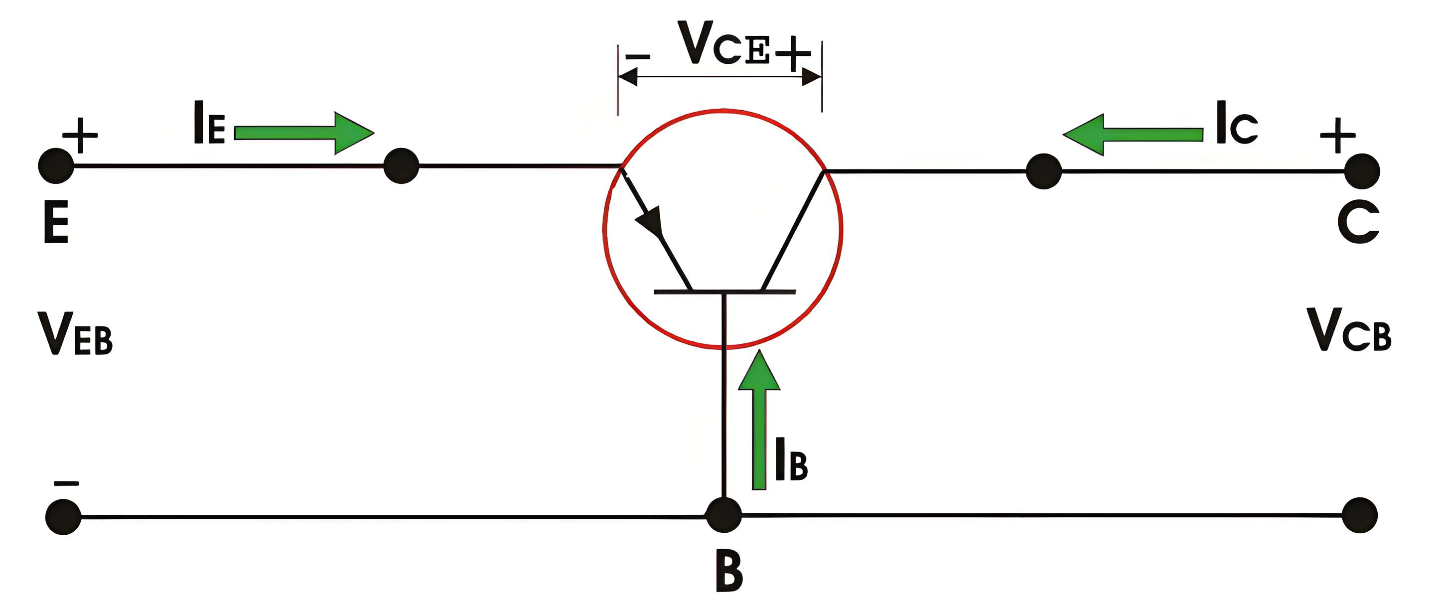
Similarly for p-n-p bipolar junction transistor (or pnp transistor), an n-type semiconductor is sandwiched between two p-type semiconductors. The diagram of a p-n-p transistor is shown below
For p-n-p transistors, current enters into the transistor through the emitter terminal. Like any bipolar junction transistor, the emitter-base junction is forward biased and the collector-base junction is reverse biased. We can tabulate the emitter, base and collector current, as well as the emitter-base, collector base and collector-emitter voltage for p-n-p transistors also.
Working Principle of BJT
The figure shows an n-p-n transistor biased in the active region (See transistor biasing), the BE junction is forward biased whereas the CB junction is reversed biased. The width of the depletion region of the BE junction is small as compared to that of the CB junction.
The forward bias at the BE junction lowers the barrier potential, allowing electrons to flow from the emitter to the base. Because the base is thin and lightly doped, it has very few holes. About 2% of the electrons from the emitter recombine with holes in the base and flow out through the base terminal.
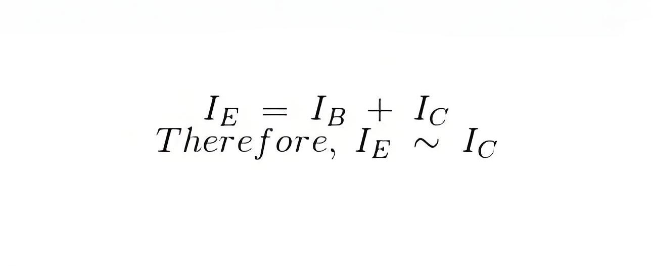
This constitutes the base current, it flows due to recombination of electrons and holes (Note that the direction of conventional current flow is opposite to that of the flow of electrons). The remaining large number of electrons will cross the reverse-biased collector junction to constitute the collector current. Thus by KCL,
The base current is very small as compared to emitter and collector current.
Here, the majority of charge carriers are electrons. The operation of a p-n-p transistor is same as of the n-p-n, the only difference is that the majority charge carriers are holes instead of electrons. Only a small part current flows due to majority carriers and most of the current flows due to minority charge carriers in a BJT. Hence, they are called as minority carrier devices.
Equivalent Circuit of BJT
A p-n junction is represented by a diode. As a transistor has two p-n junctions, it is equivalent to two diodes connected back to back. This is called as the two diode analogy of the BJT.
Bipolar Junction Transistors Characteristics
The three parts of a BJT are collector, emitter and base. Before knowing about the bipolar junction transistor characteristics, we have to know about the modes of operation for this type of transistors. The modes are
Common Base (CB) mode
Common Emitter (CE) mode
Common Collector (CC) mode
All three types of modes are shown below
Now coming to the characteristics of BJT there are different characteristics for different modes of operation. Characteristics is nothing but the graphical forms of relationships among different current and voltage variables of the transistor. The characteristics for p-n-p transistors are given for different modes and different parameters.

Common Base Characteristics
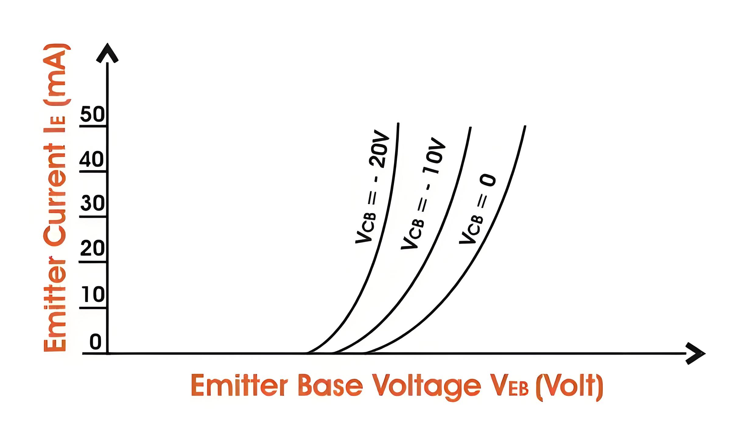
Input Characteristics
For p-n-p transistor, the input current is the emitter current (IE) and the input voltage is the collector base voltage (VCB).
As the emitter-base junction is forward biased, therefore the graph of IE Vs VEB is similar to the forward characteristics of a p-n diode. IE increases for fixed VEB when VCB increases.
Output Characteristics
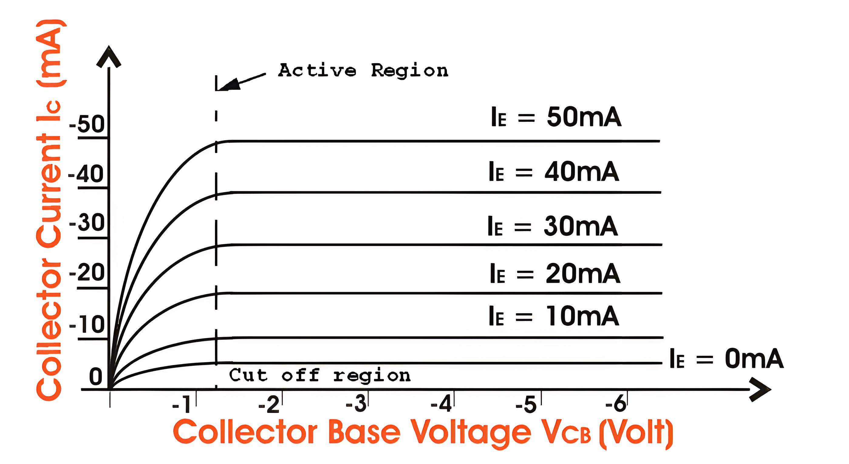
The output characteristics show the relation between the output voltage and output current IC is the output current and collector-base voltage and the emitter current IE is the input current and works as the parameters. The figure below shows the output characteristics for a p-n-p transistor in CB mode.
As we know for p-n-p transistors I E and VEB are positive and IC, IB, VCB are negative. These are three regions in the curve, active region saturation region and the cut off region. The active region is the region where the transistor operates normally.
Here the emitter junction is reverse biased. Now the saturation region is the region where both the emitter-collector junctions are forward biased. And finally, the cut off region is the region where both emitter and the collector junctions are reverse biased.
Common Emitter Characteristics
Input characteristics
IB (Base Current) is the input current, VBE (Base – Emitter Voltage) is the input voltage for CE (Common Emitter) mode. So, the input characteristics for CE mode will be the relation between IB and VBE with VCE as a parameter. The characteristics are shown below
The typical CE input characteristics are similar to that of a forward-biased of p-n diode. But as V CB increases the base width decreases.
Output Characteristics
Output characteristics for CE mode is the curve or graph between collector current (IC) and collector-emitter voltage (VCE) when the base current IB is the parameter. The characteristics is shown below in the figure.
Like the output characteristics of common – base transistor CE mode has also three regions named (i) Active region, (ii) cut-off regions, (iii) saturation region. The active region has collector region reverse biased and the emitter junction forward biased.
For cut-off region, the emitter junction is slightly reverse biased and the collector current is not totally cut-off. And finally for the saturation region both the collector and the emitter junction are forward biased.
The Electricity Encyclopedia is dedicated to accelerating the dissemination and application of electricity knowledge and adding impetus to the development and innovation of the electricity industry.

