Bipolar Junction Transistor Connections
Bipolar Junction Transistor Definition
A Bipolar Junction Transistor (BJT) is a three-terminal device. It can function as either an amplifier or a switch, requiring one input circuit and one output circuit. To handle this with only three terminals, one terminal serves as a common connection for both input and output. The choice of the common terminal depends on the application. There are three types of transistor connections: common base, common emitter, and common collector.
Common Base Transistor
Common Emitter Transistor
Common Collector Transistor.
Here one thing to be remembered that whatever may be the connection of a transistor, but the base-emitter junction must be kept forward biased and base-collector junction must be kept reverse biased.
Common Base Connection of BJT
Here the base terminal is common to both input and output circuit. The common base configurations or modes are as shown in the figure below. Here, the common base mode of npn transistor and pnp transistor are shown separately. Here emitter-base circuit is taken as input circuit and collector base circuit as output circuit.
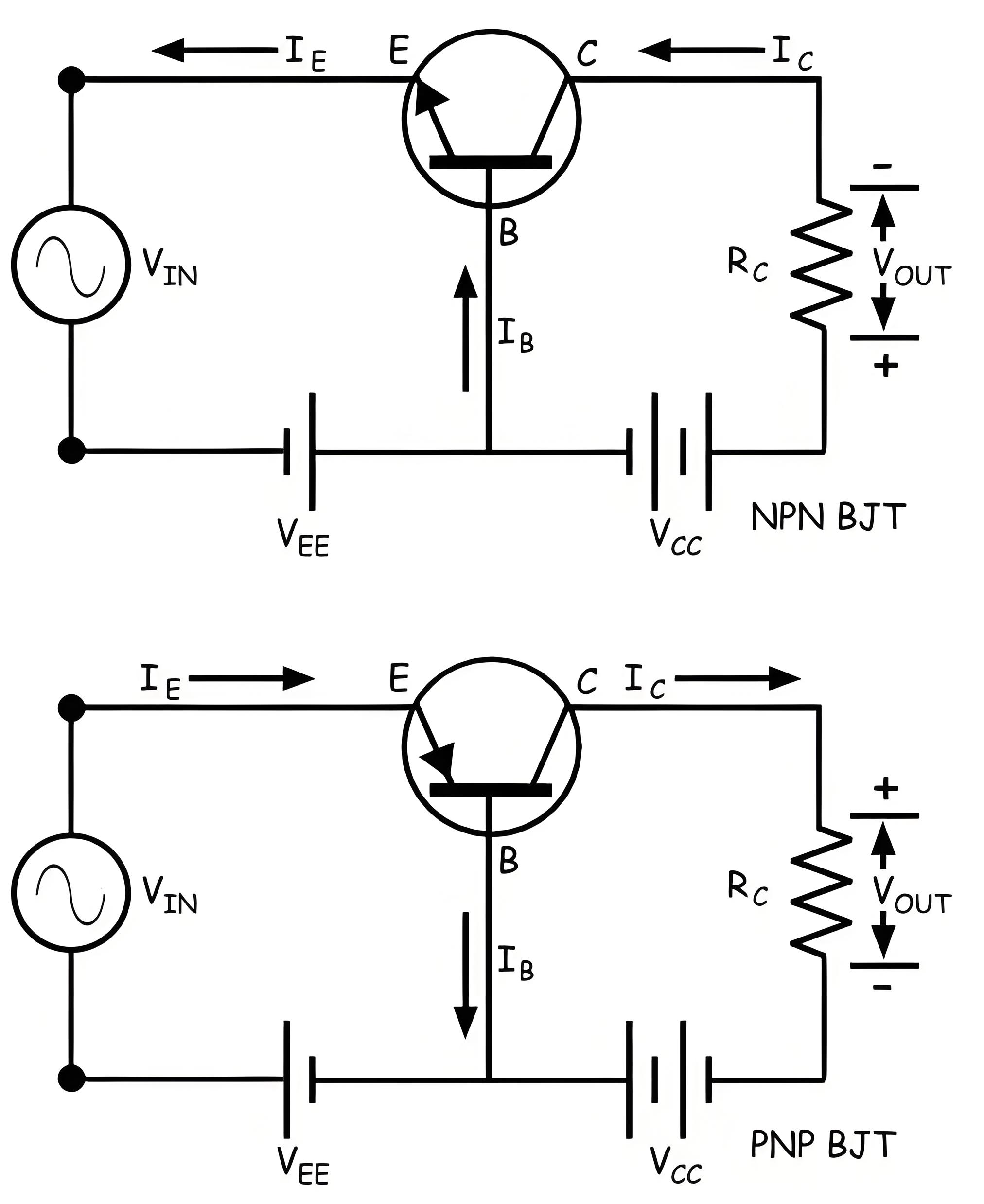
Current Gain
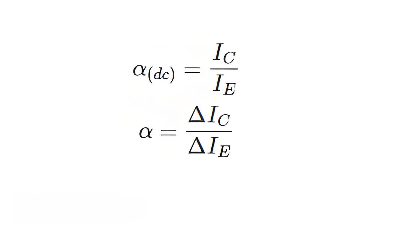
Here the input current is emitter current IE and output current is collector current IC. The current gain is considered as when we only consider the dc biasing voltages of the circuit and no alternating signal is applied in the input. Now if we consider the alternating signal applied to the input then the current amplification factor (α) at a constant collector-base voltage, would be
Here it is seen that neither of current gain and current amplification factor has value more than unity since collector current in no way can be more than emitter current. But as we know that the emitter current and collector current are nearly equal in a bipolar junction transistor, these ratios would be very near to unity. The value generally ranges from 0.9 to even 0.99.
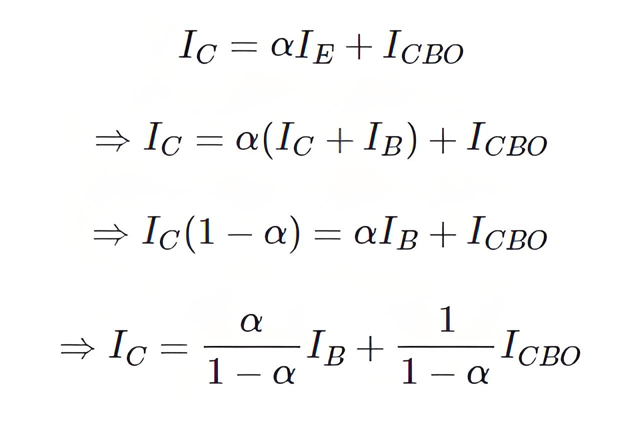
Expression of Collector Current
If the emitter circuit is open, there will be no emitter current (IC = 0). But in this condition, there will be a tiny current flowing through the collector region. This is because of flow of minority charge carriers and this is the reverse leakage current. As this current flows through collector and base keeping the emitter terminal open, the current is denoted as ICBO. In small power rated transistor the reverse leakage current ICBO is quite small and generally, we neglect it during calculations but in high power rated transistor this leakage current cannot be neglected. This current is highly dependent on the temperature so at high temperatures the reverse leakage current ICBO cannot be neglected during calculations. This expression proves that collector current also depends on base current.
Characteristic of Common Base Connection
Input Characteristic
This is drawn between input current and input voltage of the transistor itself. The input current is emitter current (IE) and the input voltage is emitter-base voltage (VEB). After crossing emitter-base junction forward barrier potential emitter current (IE) starts increasing rapidly with increasing emitter-base voltage (VEB).
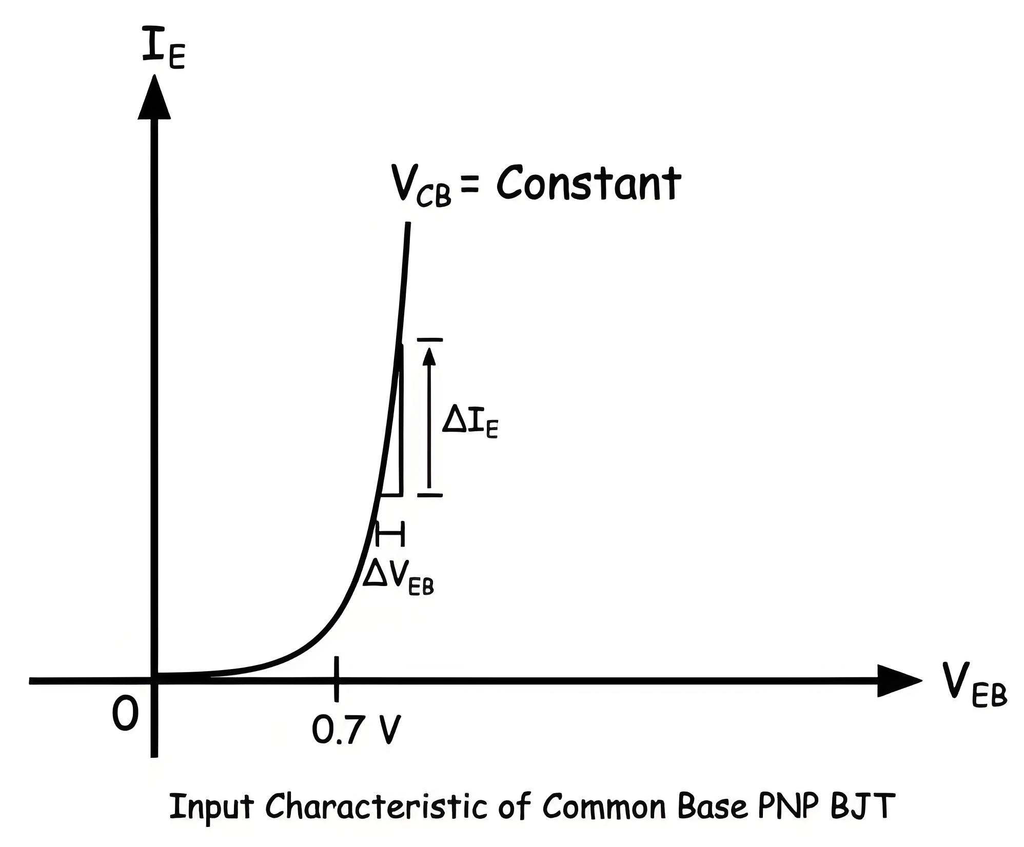
The inpur resistance of the circuit is the ratio of change in emitter-base voltage (ΔV EB) to emitter current (ΔIE) at a constant collector-base voltage (VCB = Constant). As the change in emitter current is quite large compared to the change in emitter-base voltage (ΔIE >> ΔVEB), the input resistance of the common base transistor is quite small.
Output Characteristic
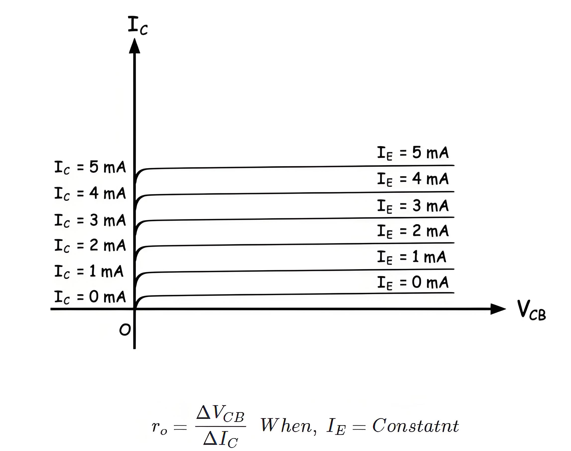
Collector current gets only constant value when there is sufficient reverse biased established between base and collector region. This is why there is a rise of collector current with an increase of collector-base voltage when this voltage has very low value. But after a certain collector-base voltage the collector-base junction gets sufficient reverse biased and hence the collector current becomes constant for a certain emitter current and it entirely depends on the emitter current.
At that situation, the entire emitter current except base current contributes the collector current. As the collector current becomes almost constant for the specified emitter current at that region of the characteristic, the increase of collector current is very very small compared to the increase of collector-base voltage.
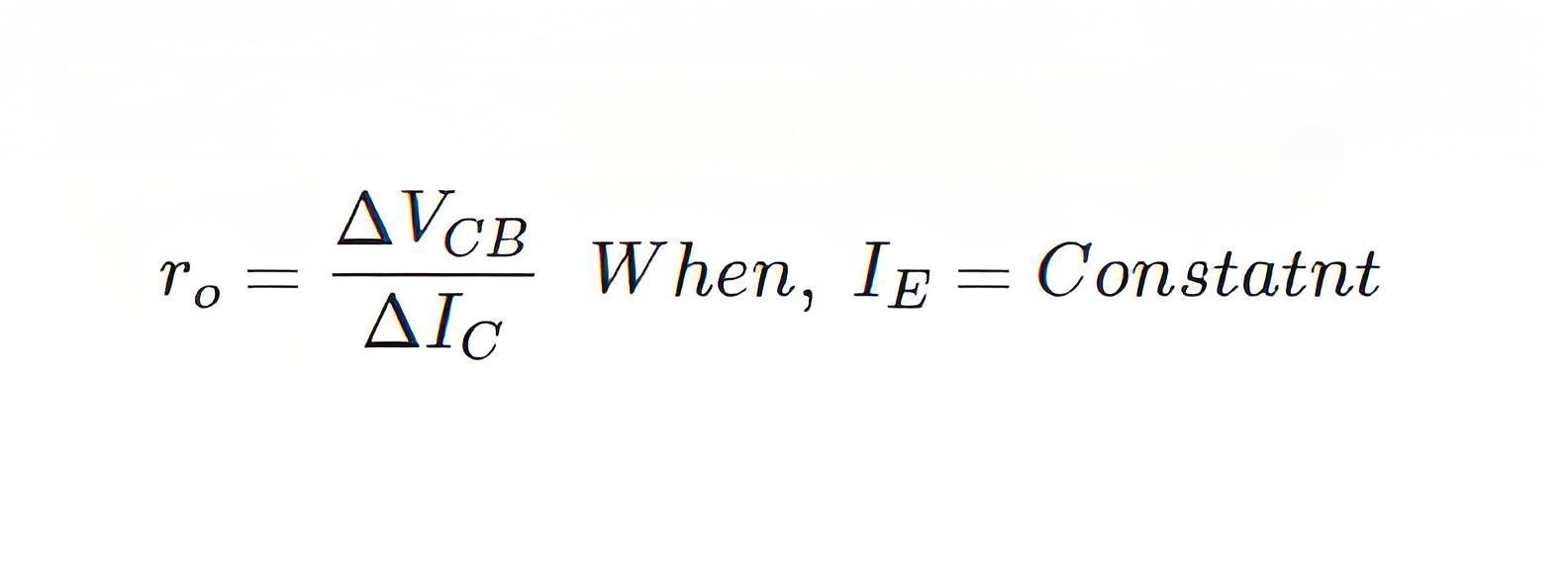
The ratio of change in collector-base voltage to the change in collector current is defined as the output resistance of common base mode of a transistor. Naturally, the value of output resistance is very high in the common base mode of a transistor.
Common Emitter Connection of BJT
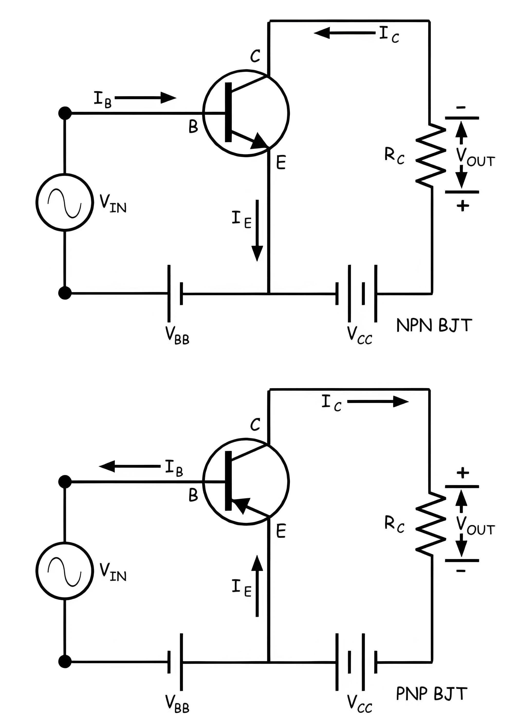
Common Emitter Transistor is the most commonly used transistor connection. Here the emitter terminal is common for both input and output circuit. The circuit connected between base and emitter is the input circuit and the circuit connected between collector and emitter is the output circuit. The common emitter mode of npn transistor and pnp transistor are shown separately in the figure below.
Current Gain
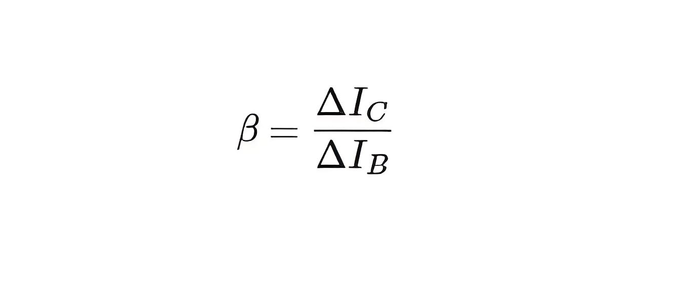
In common emitter configuration, the input current is base current (IB) and the output current is collector current (IC). In bipolar junction transistor, the base current controls the collector current. The ratio of change in collector current (ΔIC) to change in base current (ΔIB) is defined as the current gain of common emitter transistor. In a bipolar junction transistor, the emitter current (IE) is the sum of the base current (IB) and collector current (IC). If base current changes, the collector current also changes and as a result the emitter current gets also changed accordingly.
Again the ratio of change of collector current to the corresponding change in emitter current is denoted by αAs the value of base current is quite low compared to the collector current (IB << IC), the current gain in a common emitter transistor is quite high and it ranges from 20 to 500.
Characteristic of Common Emitter Transistor
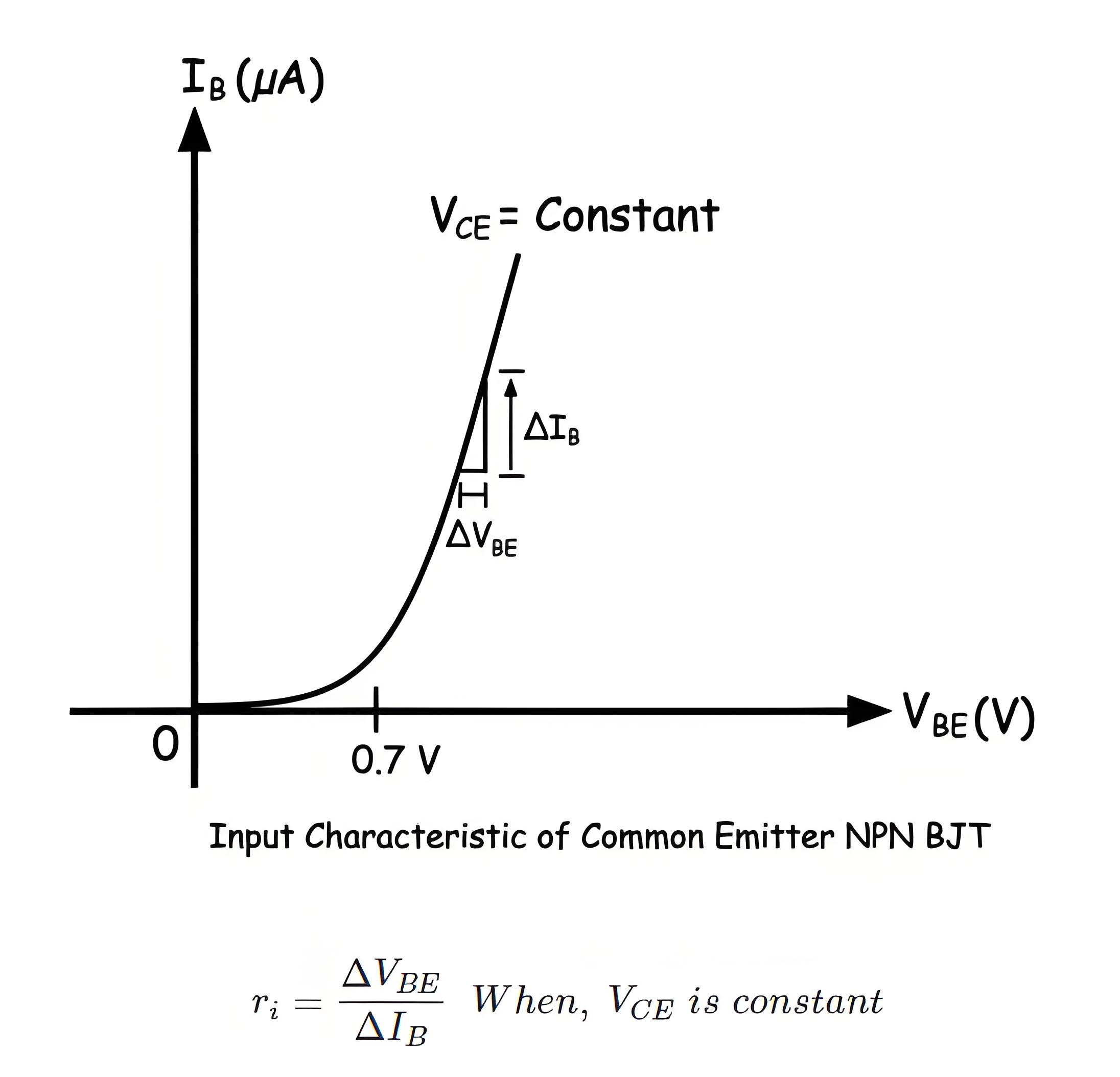
In common emitter mode of the transistor, there are two circuits – input circuit and the output circuit. In the input circuit, the parameters are base current and base-emitter voltage. The characteristic curve drawn against variations of base current and base-emitter voltage is input characteristic of a common emitter transistor. The pn junction between base and emitter is forward biased hence the characteristic would be similar to that of a forward biased pn junction diode. Here also the base current does not get any value before the base-emitter voltage crosses the forward barrier potential of the junction but after that, the base current rises significantly with the increase of base-emitter voltage. The rate of rising of base current with respect to the base-emitter voltage is high here but not as high as in the case of common base mode.
Hence input resistance of the circuit is higher than that of the common base mode of a transistor.
Output Characteristic of Common Emitter Transistor
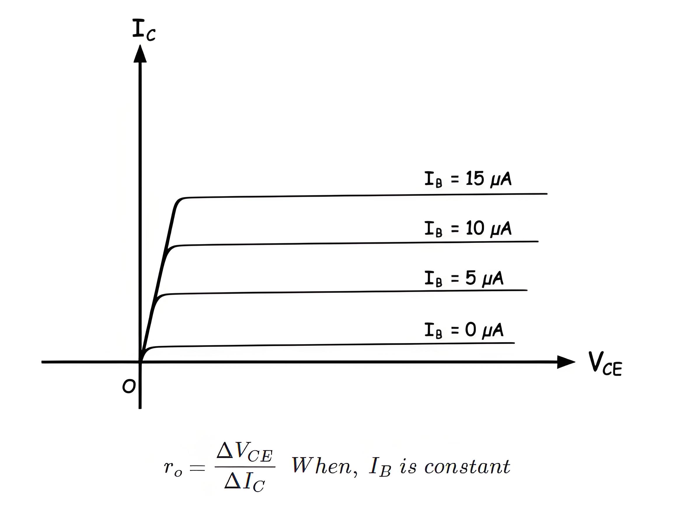
The output characteristic is drawn against variations of output current and the output voltage of the transistor. The collector current is output current and collector-emitter voltage is the output voltage of the transistor. Here the variation of collector current for different values of collector-base voltage is plotted against a fixed value of base current. It is found that at the beginning the collector current proportionately gets increased with increasing collector-emitter voltage but after certain voltage level, the collector current becomes almost constant. This is because at the beginning the base-collector junction does not get sufficient reverse biasing but after a certain voltage it becomes sufficiently reverse biased and then the major portion of charge carriers coming from emitter region to base region would migrate to collector region to contribute collector current. The number of majority carriers coming from emitter region depends on the base current in a BJT hence for a specific base current the collector current is constant.
The output resistance would be
Common Collector Connection of BJT
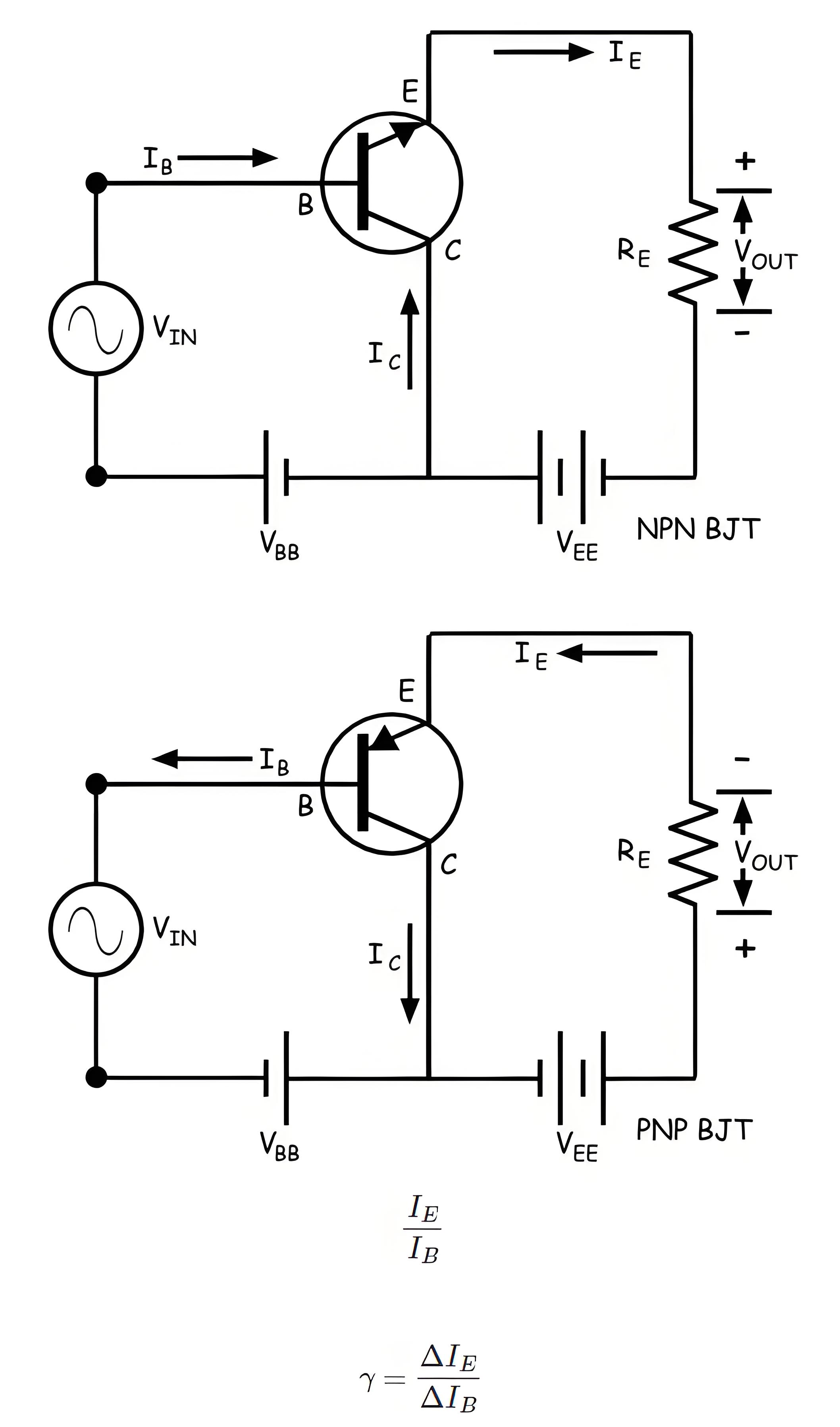
In common collector configuration the input circuit is between base and collector terminal and the output circuit is between emitter and collector terminal.
The ratio of change of emitter current to change of base current is defined as the current gain of common collector configuration. This is denoted as,
The current amplification factor of the circuit is the ratio of change of emitter current to change of base current when a time-varying signal is applied to the input.
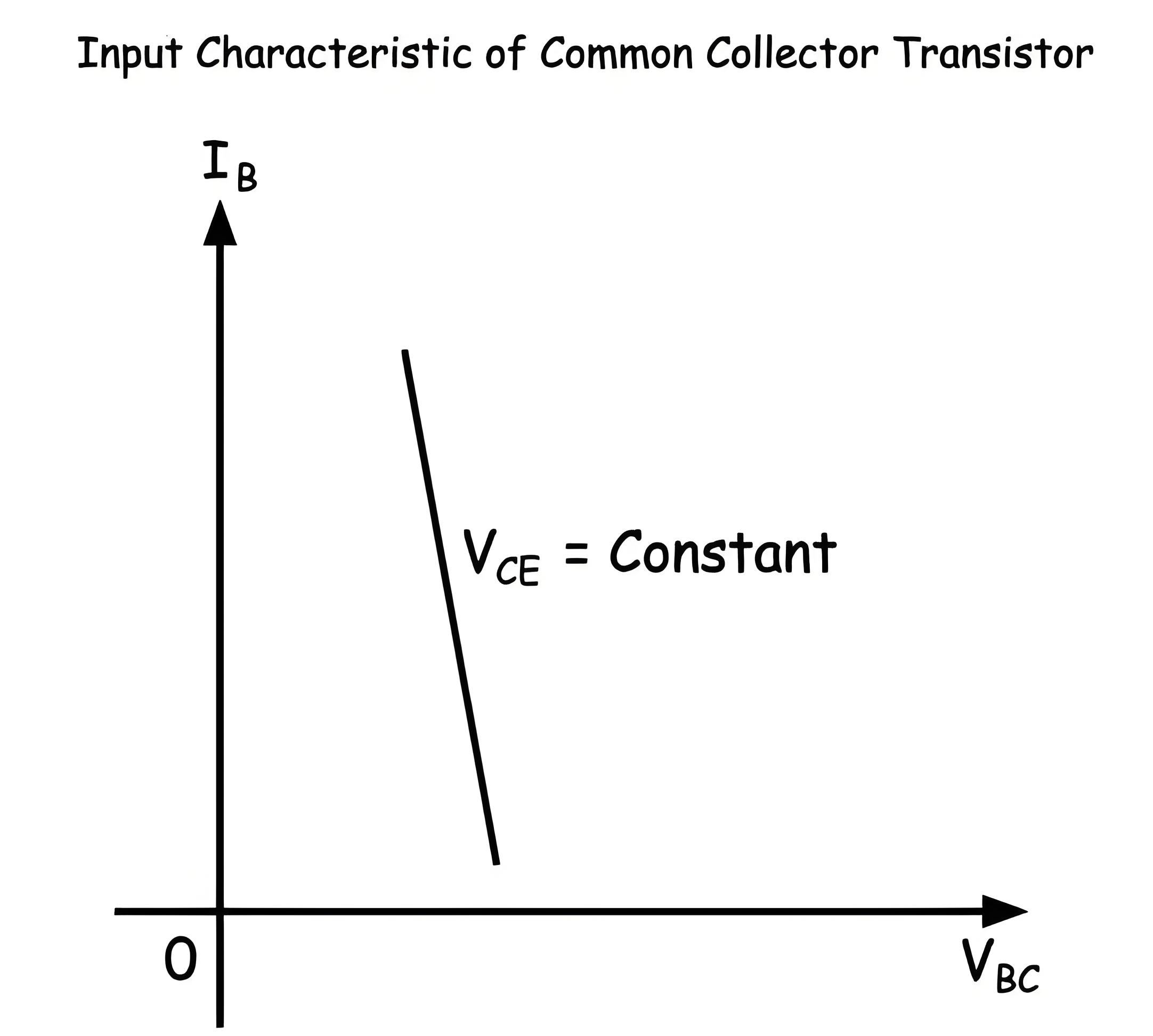
Input Characteristic of Common Collector Transistor
The input current is base current and input voltage of the transistor is base-collector voltage. The base-collector junction is reverse biased and hence with increasing base-collector voltage the reverse biasing of the junction increases. This causes base current to decrease slightly with the increase in base-collector voltage. Since at this condition more minority carriers of the base region will propagate to collector region and hence electron-hole recombination rate would get decreased in the base region causing a decrement in base current.
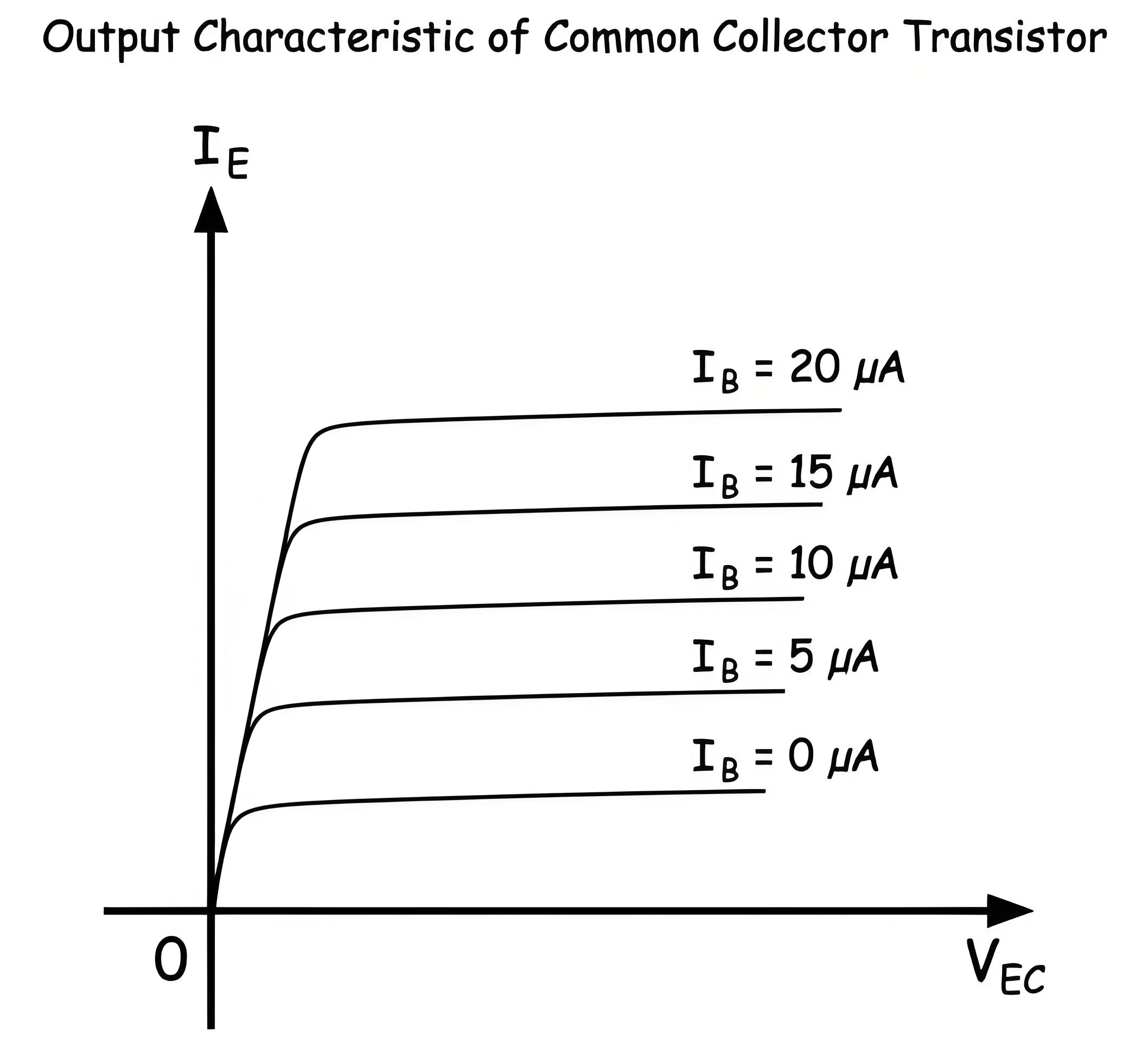
Output Characteristic of Common Collector Transistor
The output characteristic of a common collector transistor is nearly the same as the output characteristic of a common emitter transistor. The only difference that here in the case of common collector configuration the output current is emitter current instead of collector current as in the case of common emitter configuration. Here also for a fixed base current, the emitter current increases linearly with increasing collector-emitter voltage up to a certain level of this voltage and then the emitter current gets almost constant irrespective of collector-emitter voltage. Although there would be a very slow increase of emitter current with the collector-emitter voltage as shown in the characteristic curve below.
The Electricity Encyclopedia is dedicated to accelerating the dissemination and application of electricity knowledge and adding impetus to the development and innovation of the electricity industry.


