RLC Circuit Analysis (Series And Parallel)
In an RLC circuit, the most fundamental elements of a resistor, inductor, and capacitor are connected across a voltage supply. All of these elements are linear and passive in nature. Passive components are ones that consume energy rather than producing it; linear elements are those which have a linear relationship between voltage and current.
There are number of ways of connecting these elements across voltage supply, but the most common method is to connect these elements either in series or in parallel. The RLC circuit exhibits the property of resonance in same way as LC circuit exhibits, but in this circuit the oscillation dies out quickly as compared to LC circuit due to the presence of resistor in the circuit.
When a resistor, inductor and capacitor are connected in series with the voltage supply, the circuit so formed is called series RLC circuit.
Since all these components are connected in series, the current in each element remains the same,

Let VR be the voltage across resistor, R.
VL be the voltage across inductor, L.
VC be the voltage across capacitor, C.
XL be the inductive reactance.
XC be the capacitive reactance.
The total voltage in the RLC circuit is not equal to the algebraic sum of voltages across the resistor, the inductor, and the capacitor; but it is a vector sum because, in the case of the resistor the voltage is in-phase with the current, for inductor the voltage leads the current by 90o and for capacitor, the voltage lags behind the current by 90o (as per ELI the ICE Man).
So, voltages in each component are not in phase with each other; so they cannot be added arithmetically. The figure below shows the phasor diagram of the series RLC circuit. For drawing the phasor diagram for RLC series circuit, the current is taken as reference because, in series circuit the current in each element remains the same and the corresponding voltage vectors for each component are drawn in reference to common current vector.

The Impedance for a Series RLC Circuit

The impedance Z of a series RLC circuit is defined as opposition to the flow of current due circuit resistance R, inductive reactance, XL and capacitive reactance, XC. If the inductive reactance is greater than the capacitive reactance i.e XL > XC, then the RLC circuit has lagging phase angle and if the capacitive reactance is greater than the inductive reactance i.e XC > XL then, the RLC circuit have leading phase angle and if both inductive and capacitive are same i.e XL = XC then circuit will behave as purely resistive circuit.
We know that
Where,
Substituting the values![]()
Parallel RLC Circuit
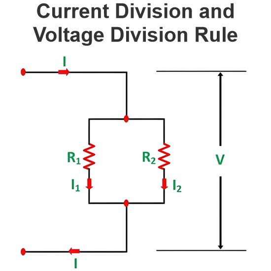
In parallel RLC Circuit the resistor, inductor and capacitor are connected in parallel across a voltage supply. The parallel RLC circuit is exactly opposite to the series RLC circuit. The applied voltage remains the same across all components and the supply current gets divided.
The total current drawn from the supply is not equal to mathematical sum of the current flowing in the individual component, but it is equal to its vector sum of all the currents, as the current flowing in resistor, inductor and capacitor are not in the same phase with each other; so they cannot be added arithmetically.
Phasor diagram of parallel RLC circuit, IR is the current flowing in the resistor, R in amps.
IC is the current flowing in the capacitor, C in amps.
IL is the current flowing in the inductor, L in amps.
Is is the supply current in amps.
In the parallel RLC circuit, all the components are connected in parallel; so the voltage across each element is same. Therefore, for drawing phasor diagram, take voltage as reference vector and all the other currents i.e IR, IC, IL are drawn relative to this voltage vector. The current through each element can be found using Kirchhoff’s Current Law, which states that the sum of currents entering a junction or node is equal to the sum of current leaving that node.

As shown above in the equation of impedance, Z of a parallel RLC circuit; each element has reciprocal of impedance (1 / Z) i.e. admittance, Y. So in parallel RLC circuit, it is convenient to use admittance instead of impedance.
Resonance in RLC Circuit
In a circuit containing inductor and capacitor, the energy is stored in two different ways.
When a current flows in a inductor, energy is stored in magnetic field.
When a capacitor is charged, energy is stored in static electric field.
The magnetic field in the inductor is built by the current, which gets provided by the discharging capacitor. Similarly, the capacitor is charged by the current produced by collapsing magnetic field of inductor and this process continues on and on, causing electrical energy to oscillate between the magnetic field and the electric field. In some cases at certain a certain frequency known as the resonant frequency, the inductive reactance of the circuit becomes equal to capacitive reactance which causes the electrical energy to oscillate between the electric field of the capacitor and magnetic field of the inductor. This forms a harmonic oscillator for current. In RLC circuit, the presence of resistor causes these oscillation s to die out over period of time and it is called as the damping effect of resistor.
Formula for Resonant Frequency
During resonance, at certain frequency called resonant frequency, fr.
When resonance occurs, the inductive reactance of the circuit becomes equal to capacitive reactance, which causes the circuit impedance to be minimum in case of series RLC circuit; but when resistor, inductor and capacitor are connected in parallel, the circuit impedance becomes maximum, so the parallel RLC circuit is sometimes called as anti-resonator. Note that the lowest resonant frequency of a vibrating object is known as its fundamental frequency
Difference between Series RLC Circuit and Parallel RLC Circuit
| S.NO | RLC SERIES CIRCUIT | RLC PARALLEL CIRCUIT |
| 1 | Resistor, inductor and capacitor are connected in series | Resistor, inductor and capacitor are connected in parallel |
| 2 | Current is same in each element | Current is different in all elements and the total current is equal to vector sum of each branch of current i.e Is2 = IR2 + (IC – IL)2 |
| 3 | Voltage across all the elements is different and the total voltage is equal to the vector sum of voltages across each component i.e Vs2 = VR2 + (VL – VC)2 | Voltage across each element remains the same |
| 4 | For drawing phasor diagram, current is taken as reference vector | For drawing phasor diagram, voltage is taken as reference vector |
| 5 | Voltage across each element is given by : VR= IR, VL = I XL, VC = I XC | Current in each element is given by: IR = V / R , IC = V / XC , IL = V / XL |
| 6 | Its more convenient to use impedance for calculations | Its more convenient to use admittance for calculations |
| 7 | At resonance , when XL = XC, the circuit has minimum impedance | At resonance, when XL = XC, the circuit has maximum impedance |
Equation of RLC Circuit
Consider a RLC circuit having resistor R, inductor L, and capacitor C connected in series and are driven by a voltage source V. Let Q be the charge on the capacitor and the current flowing in the circuit is I. Apply Kirchhoff’s voltage law
![]()
In this equation; resistance, inductance, capacitance and voltage are known quantities but current and charge are unknown quantities. We know that an current is a rate of electric charge flowing, so it is given by![]()
Differentiating again I'(t) = Q’’ (t)![]()
Differentiating the above equation with respect to ’t’ we get,![]()
Now at time t = 0, V(0) = 0 and at time t = t, V(t) = Eosinωt
Differentiating with respect to ’t’ we get V'(t) = ωEocosωt
Substitute the value of V'(t) in above equation![]()
Let us say that the solution of this equation is IP(t) = Asin(ωt – ǿ) and if IP(t) is a solution of above equation then it must satisfy this equation,![]()
Now substitute the value of IP(t) and differentiate it we get,
Apply the formula of cos (A + B) and combine similar terms we get,![]()
Match the coefficient of sin(ωt – φ) and cos(ωt – φ) on both sides we get,![]()
Now we have two equations and two unknowns i.e φ and A, and by dividing the above two equations we get,![]()
Squaring and adding above equation, we get
Analysis of RLC Circuit Using Laplace Transformation
Step 1 : Draw a phasor diagram for given circuit.
Step 2 : Use Kirchhoff’s voltage law in RLC series circuit and current law in RLC parallel circuit to form differential equations in the time-domain.
Step 3 : Use Laplace transformation to convert these differential equations from time-domain into the s-domain.
Step 4 : For finding unknown variables, solve these equations.
Step 5 : Apply inverse Laplace transformation to convert back equations from s-domain into time domain.
Statement: Respect the original, good articles worth sharing, if there is infringement please contact delete.
Electrical4U is dedicated to the teaching and sharing of all things related to electrical and electronics engineering.


