What is Photovoltaic Effect?
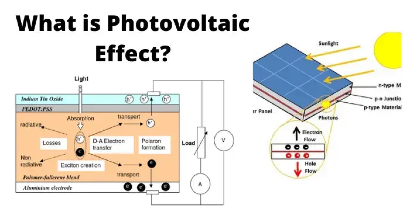
The effect due to which light energy is converted to electric energy in certain semiconductor materials is known as photovoltaic effect. This directly converts light energy to electricity without any intermediate process. For demonstrating the photovoltaic effect let us assume a block of silicon crystal.
The upper portion of this block is doped with donor impurities and lower portion is doped with accept or impurities. Hence the concentration of free electrons is quite high in n-type region compared to p-type region and concentration of hole is quite high in p-type region compared to n-type region of the block. There will be a high concentration gradient of charge carriers across the junction line of the block. Free electrons from n-type region try to diffuse to p-type region and holes in p-type region try to diffuse to n-type region in the crystal. This is because charge carriers by nature always tend to diffuse from high concentration region to low concentration region. Each free electron of n-type region while comes to the p-type region due to diffusion, it leaves a positive donor ion behind it in the n-type region.
This is because each of the free electron in n-type region is contributed by one neutral donor atom. Similarly when a hole is diffused from p-type region to n-type region, it leaves a negative accept or ion behind it in p-type region.
Since each hole is contributed by one acceptor atom in p-type region. Both of these ions i.e. donor ions and acceptor ions are immobile and fixed at their position in crystal structure. It is needless to say that those free electrons of n-type region which are nearest to the p-type region first diffuse in the p-type region consequently create a layer of positive immobile donor ions in the n-type region adjacent to the junction.

Similarly those free holes of p-type region which are nearest to the n-type region first diffuse in the n-type region consequently create a layer of negative immobile acceptor ions in the p-type region adjacent to the junction. These positive and negative ions concentration layer creates an electric field across the junction which is directed from positive to negative that in from n-type side to p-type side. Now due to presence of this electric field charge carriers in the crystal experience a force to drift according to the direction of this electric field. As we know the positive charge always drift in the direction of electric field hence the positively charged holes (if any) in n-type region now drift to the p-side of the junction.
On the other hand, negatively charged electrons in p-type region (if any) drift to n-region as negative charge always drift opposite to the direction of electric field. Across a p-n junction diffusion and drift of charge carriers continues. Diffusion of charge carriers creates and increases the thickness of the potential barrier across the junction and drift of the charge carriers reduces the thickness of the barrier. In normal thermal equilibrium condition and in absence of any external force, the diffusion of charge carrier is equal and opposite of drift of charge carriers hence the thickness of potential barrier remains fixed.
Now the n-type surface of the silicon crystal block is exposed to the sunlight. Some of the photons are absorbed by the silicon block. Some of the absorbed photon will have energy greater than the energy gap between valence and conduction band of valence electrons of the silicon atoms. Hence, some of the valence electrons in the covalent bond will be excited and jump out from the bond leaving behind a hole in the bond. In this way electron-hole pairs are generated in the crystal due to incident light. The holes of these light generated electron-hole pairs in the n-type side have enough probability of recombination with enormous electrons (majority carriers). Hence, solar cell is so designed, that the light- generated electrons or holes will not get enough chances to recombine with majority carriers.
The semiconductor (silicon) is so doped that the p-n junction forms in very close vicinity of exposed surface of the cell. If an electron hole pair is created within one minority carrier diffusion length, of the junction, the electrons of electron-hole pair will drift toward n-type region and hole of the pair will swept to p region due to in influence of electric field of the junction and hence on the average, it will contribute to current flow in an external circuit.
Statement: Respect the original, good articles worth sharing, if there is infringement please contact delete.
Electrical Operations provides detailed insights into safe and efficient electrical procedures, guiding practitioners through every step of handling electrical systems.
