Schmitt Trigger: What is it And How Does it Work?
What is a Schmitt Trigger?
A Schmitt Trigger is a comparator circuit with hysteresis implemented by applying positive feedback to the noninverting input of a comparator or differential amplifier. A Schmitt Trigger uses two input different threshold voltage level to avoid noise in the input signal. The action from this dual-threshold is known as hysteresis.
The Schmitt Trigger was invented by American scientist Otto H Schmitt in 1934.
The normal comparator contains only one threshold signal. And it compares the threshold signal with an input signal. But, if the input signal has noise, it may affect the output signal.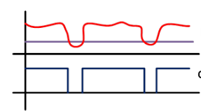
In the above figure, because of the noise at locations A and B, the input signal (V1) crosses the level of the reference signal (V2). During this period, the V1 is less than V2 and the output is low.
Hence, the output of the comparator is affected by the noise in the input signal. And the comparator is not protected from the noise.
The “trigger” in the name “Schmitt Trigger” comes from the fact that the output retains its value until the input varies sufficiently to “trigger” a change.
How does a Schmitt Trigger work?
The Schmitt trigger gives proper results even if the input signal is noisy. It uses two threshold voltages; one is the upper threshold voltage (VUT) and the second is lower threshold voltage (VLT).
The output of the Schmitt trigger remains low until the input signal crosses VUT. Once the input signal cross this limit VUT, the output signal of the Schmitt trigger remains high until the input signal is below the level of VLT.
Let’s understand the working of Schmitt trigger with an example. Here we assume that the initial input is zero.
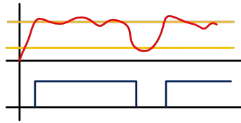
Noise effect with Schmitt Trigger
Here, we have assumed that the initial input signal is zero and it increases gradually as shown in the above figure.
The output signal of the Schmitt trigger remains low until point A. At point A, the input signal crosses above the level of the upper threshold (VUT) and it makes a high output signal.
The output signal remains high until point B. At point B, the input signal crosses below the lower threshold. And this makes the output signal low.
And again, at point C, when the input signal crosses above the upper threshold, the output is high.
In this condition, we can see that the input signal is noisy. But the noise is not affected in the output signal.
Schmitt Trigger Circuit
The Schmitt trigger circuit uses positive feedback. Therefore, this circuit is also known as the regenerative comparator circuit. The Schmitt Trigger circuit can be designed with the help of Op-Amp and Transistor. And it classified as;
Op-amp based Schmitt trigger
Transistor based Schmitt trigger
Op-Amp based Schmitt Trigger
The Schmitt trigger circuit can be designed using Op-Amp in two ways. If the input signal is connected at the inverting point of Op-Amp, it is known as Inverting Schmitt Trigger. And if the input signal is connected at the non-inverting point of Op-Amp, it is known as Non-inverting Schmitt Trigger.
Inverting Schmitt Trigger
In this type of Schmitt trigger, the input is given at the inverting terminal of op-amp. And the positive feedback from output to input.
Now, let’s understand how this circuit works. At point A, the voltage is V and the applied voltage (input voltage) is Vin.If the applied voltage Vin is greater than V, the output of the circuit will be low. And if the applied voltage Vin is less than V, the output of the circuit will be high.
Now, calculate the equation of V.
Applying Kirchhoff’s Current Law (KCL),
Now, let’s assume that the output of the Schmitt trigger is high. In this condition,
So, from the above equation;
When the input signal is greater than the V1, the output of the Schmitt trigger will become low. Hence, V1 is an upper threshold voltage (VUT).
The output will remain low until the input signal is less than V. when the output of the Schmitt trigger is low, in this condition,
Now, the output remains high until the input signal is less than V2. Hence, the V2 is known as a lower threshold voltage (VLT).
Non-Inverting Schmitt Trigger
In non-inverting Schmitt trigger, the input signal is applied at the non-inverting terminal of Op-Amp. And positive feedback is applied from output to input. The inverting terminal of Op-Amp is connected to the ground terminal. The circuit diagram of the non-inverting Schmitt trigger is as shown below figure.
In this circuit, the output of the Schmitt trigger will high when voltage V is greater than zero. And the output will low when voltage V is less than zero.
Now, let’s find the equation of voltage V. For that, we apply KCL at that node.
Now, assume that the output of Op-Amp is low. Hence, the output voltage of the Schmitt trigger is VL. And voltage V is equal to V1.
In this condition,
From the above equation,
When the voltage V1 is greater than zero, the output will high. In this condition,
When the above condition is satisfied, the output will high. therefore, this equation gives the value of the upper threshold voltage (VUT).
Now assume that the output of the Schmitt trigger is high. And the voltage V is equal to V2.
From the equation of voltage V.
The output of the Schmitt trigger will become low when the voltage V2 is less than zero. In this condition,
The above equation gives the value of the lower threshold voltage (VLT).
Transistor based Schmitt Trigger
The Schmitt trigger circuit can be designed with the help of two transistors. The circuit diagram of the transistor-based Schmitt trigger is given in the below circuit.
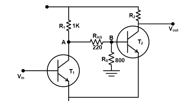
Vin = input voltage
Vref = Reference voltage = 5V
Let’s assume that, at starting, an input voltage Vin is zero. The input voltage is given to the base of transistor T1. Hence, in this condition, the transistor T1 operates in the cut-off region and it remains non conducting.
Va and Vb are node voltage. The reference voltage is given 5V. So, we can calculate the value of Va and Vb by the voltage divider rule.
Voltage Vb is given to the base of transistor T2. And it is 1.98V. Therefore, the transistor T2 is conducting. And due to this, the output of the Schmitt trigger is low. The drop at an emitter is about 0.7V. So, the base of the transistor voltage is 1.28V.
The emitter of transistor T2 is connected with the emitter of transistor T1. Hence, both transistors operate at the same level at 1.28V.
It means that the transistor T1 will operate when the input voltage is 0.7V above 1.28V or more than 1.98V (1.28V + 0.7V).
Now, we increase the input voltage more than 1.98V, and transistor T1 will start conducting. This causes the voltage drop of the base of transistor T2 and it will cut off the transistor T2. And due to this, the output of the Schmitt trigger is high.
The input voltage starts decreasing. The transistor T1 will cut off when the input voltage is 0.7V less than 1.98V and it is 1.28V. In this condition, the transistor T2 gets sufficient voltage from the reference voltage, and it will turn on. This makes the output of Schmitt trigger low.
Therefore, in this condition, we have two thresholds, a lower threshold at 1.28V and a higher threshold at 1.98V.
Schmitt Trigger Oscillator
The Schmitt Trigger can be used as an oscillator by connecting a single RC integrated circuit. The circuit diagram of the Schmitt trigger oscillator is as shown in the below figure.
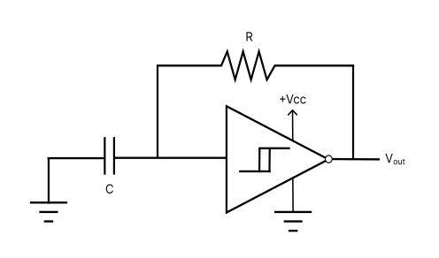
The output of the circuit is a continuous square wave. And the frequency of the waveform depends on the value of R, C, and threshold point of Schmitt Trigger.
Where k is a constant and it ranges between 0.2 and 1.
CMOS Schmitt Trigger
The simple signal inverter circuit gives the opposite output signal from the input signal. For example, if the input signal is high, the output signal is low for a simple inverter circuit. But if the input signal has spikes (noise), the output signal will react change on a spike. That we don’t want. Therefore, the CMOS Schmitt trigger is used.
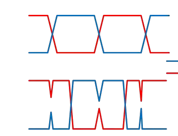
In the first waveform, the input signal has no noise. So, the output is perfect. But in the second figure, the input signal has some noise. The output is also reacting to this noise. To avoid, this condition, CMOS Schmitt trigger is used.
The below circuit diagram shows the construction of the CMOS Schmitt trigger. The CMOS Schmitt Trigger consists of 6 transistors including PMOS and NMOS transistors.
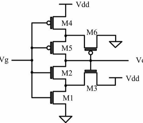
First, we need to know, what is PMOS and NMOS transistor? The symbol of PMOS and NMOS transistors are in the below figure.
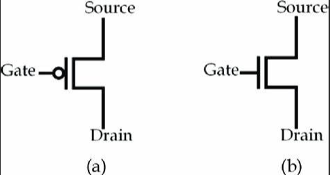
NMOS transistor conducts when VG is greater than VS or VD. And PMOS transistor conducts when VG is less than VS or VD. In CMOS Schmitt trigger, one PMOS and one NMOS transistors are added in a simple inverter circuit.
In the first case, the input voltage is high. In this condition, the PN transistor is ON and the NN transistor is OFF. And it creates a path to ground for node-A. Therefore, the output of the CMOS Schmitt trigger will be zero.
In the second case, the input voltage is high. In this condition, the NN transistor is ON and the PN transistor is OFF. It will create a path to voltage VDD (High) for node-B. Therefore, the output of the CMOS Schmitt trigger will be high.
Schmitt Trigger Applications
The applications of Schmitt trigger are as below.
Schmitt trigger is used to a sine wave and triangular wave into square waves.
The most important use of the Schmitt triggers to remove noise in the digital circuit.
It is also used as a function generator.
It is utilized to implement an oscillator.
Schmitt triggers with the RC circuit is used as switch debouncing.
Source: Electrical4u.
Statement: Respect the original, good articles worth sharing, if there is infringement please contact delete.
Electrical4U is dedicated to the teaching and sharing of all things related to electrical and electronics engineering.

