Explain Diode and it’s Types
What is a Diode?
Diodes are two-terminal electrical devices that act as a one-way switch, allowing current to flow (transfer) only in one direction. These diodes are made from semiconductor materials such as
Silicon,
Germanium, and
Gallium arsenide.
The diode’s two terminals are referred to as the Anode and Cathode. The functioning of a diode may be categorised into two types based on the potential difference (potential energy) between these two terminals:
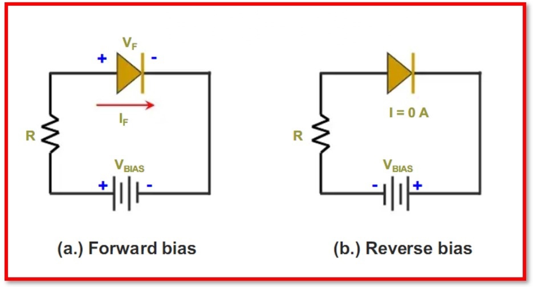
If the anode has a greater voltage than the cathode, the diode is considered to be in Forward Bias & current can flow.
If the cathode has a greater voltage than the anode, the diode is said to be in Reverse Bias, and current cannot flow.
Various kinds of diodes need different voltages.
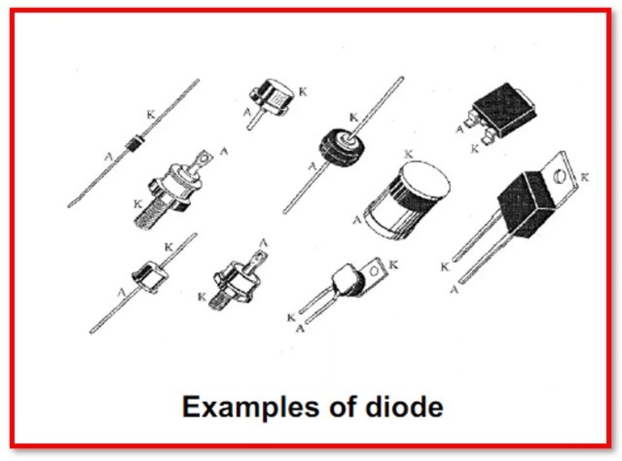
The forward voltage of silicon diodes is 0.7V, whereas that of germanium diodes is 0.3V.
When working with Silicon Diodes, the cathode terminal is often indicated by the black band or dark band on one end of the diode, while the anode terminal is typically shown by the other terminal.
Rectification, or converting AC to DC, is one of the most common applications of diodes.
Diodes are utilised in reverse polarity protector & transient protector applications because they allow current to flow (pass through) only in one direction and inhibit current flow in the other.
Symbol of Diode
A diode symbol is illustrated below. Under the forward biased condition, the arrow-head points (indicates) in the direction of conventional current flow. That is, the anode is linked to the p side & the cathode to the n side.
A simple PN junction diode by doping a silicon or germanium crystal block with pentavalent (or) donor impurity in one section & trivalent (or) acceptor impurity in the other.

A PN junction may also be formed by linking a p-type and an n-type semiconductor together using a particular manufacturing process. The anode is the terminal connecting to the p-type. The cathode is the terminal connecting to the n-type side.
At the center of the block, these dopings form a PN junction.
Working Principle of a Diode
The interaction between n-type and p-type semiconductors is the fundamental process behind the operation of a diode.
An n-type semiconductor consists of many (large) number of free electrons & minor (small) number of holes. In other terms, in an n-type semiconductor, the concentration of free electrons is large while the concentration of holes is quite low.
In an n-type semiconductor, free electrons are referred (known) to as majority charge carriers, whereas holes are referred to as minority charge carriers.
A p-type semiconductor is characterised by having a high number of holes relative to the amount of free electrons it contains. Holes constitute the vast majority of charge carriers in a p-type semiconductor, whereas free electrons represent only a minor portion of this kind of charge carriers .
Characteristics of Diode
Forward biased diode
Reverse biased diode
Unbiased biased diode (Zero biased) diode
1). Forward biased diode
There is a small decrease in voltage across the diode when it is biased in the forward direction and current is passing through it.
The forward voltage of germanium diodes is 300 mV, which is much lower than the forward voltage of silicon diodes, which is 690 mV.
The potential energy across p-type material is positive, whereas the potential energy across n-type material is negative. p-type materials have a positive potential energy.
2). Reverse Biased Diode
When the voltage of the battery is brought all the way down to zero, a diode is said to have a reverse bias. The reverse voltage for germanium diodes is -50(μA) microamperes, while the reverse voltage for silicon diodes is -20(μA) microamperes. When view across a p-type material, the potential energy is negative, but when view across an n-type material, the potential energy is positive.
3). Un-biased Diode (Zero Biased Diode)
It is stated that a diode has a zero-bias condition when the voltage potential that is measured across the diode is zero.
Applications of Diode
Protection against a current flowing in the reverse direction using diodes
Diodes are often used in circuits that clamp (clamping circuits).
Diode use in logic gate circuitry
Diodes are a common component in clipping circuits.
Rectification devices comprised of diodes
Types of Diode
1). Backward Diode
2). BARITT Diode
3). Gunn Diode
4).Laser Diode
5). Light Emitting Diode
6). Photodiode
7). PIN Diode
8). Fast Recovery Diode
9). Step Recovery Diode
10). Tunnel Diode
11). P-N Junction Diode
12). Zener Diode
13).Schottky Diodes
14). Shockley Diodes
15). Varactor (or)Vari-cap Diode
16). Avalanche Diode
17). Constant-current Diode
18). Gold Doped Diodes
19). Super Barrier Diodes
20). Peltier Diode
21). Crystal Diode
22). Vaccuum Diode
23). Small Signal Diode
24). Large Signal Diode
1). Backward Diode
This kind of diode is also known as a “back diode,” and it is not used very often. The backward (back) diode is a PN-junction diode, which works like a tunnel diode. Quantum tunnelling is an important part of how the current flows, especially in the opposite direction. With the energy band picture, you can see exactly how the diode works.

The band at the top level is called the “conduction band,” and the band at the bottom level is called the “valency band.” When energy is added to electrons, they tend to get more energy & move towards the conduction band. When electrons move from the valence band to the conduction band, they leave holes in the valence band.
In the zero-biasing state, the valency band that is occupied is opposite to the conduction band that is occupied. In reverse bias condition, on the other hand, the N-region moves up while the P-region moves down. Now, the band that is complete in P-section is different from the band that is empty in the N-section. So, electrons start to move from the full band in P-section to the empty band in the N-section by tunnelling.
So, this implies that current flow occurs even when the bias is in the opposite direction. In forward bias condition, the N-region moves in the same direction as the P-region, which is up. Now, the band that is filled in the N-section is different from the band that is empty in the P-section. So, electrons start to move from the full band in the N-section to the empty band in the P-section by tunnelling.
In this kind of diode, the negative (-) resistance region is formed, which is the main part of the diode that makes it work.
2). BARITT Diode
This kind of diode is also known by its extended term, which is Barrier Injection Transit Time diode, or BARRITT diode. It is suitable in microwave applications & enables various comparisons to be made to the IMPATT diode, which is utilised more commonly.
The use of thermal energy is that causes the emission from this particular kind of diode. When compared to other types of diodes, this one produces far less noise.
Mixers, amplifiers or oscillators are some of the possible applications for these given their small-signal capacity. They may also be used in a variety of other devices.
3). Gunn Diode
A PN junction diode, also known as a Gunn diode, is a kind of diode that is a type of semiconductor device that consists of two terminals. In most applications, it is used in the production of microwave signals.
Oscillators developed from Gunn diodes are used wherever there is a need for radio transmission.
They are also used in military organizations This diode is an essential component of all tachometers, even the most basic ones. Gunn diodes may make it easy to include door-opening sensor technology in modern monitoring systems, which is a need in modern monitoring systems. Moreover, this diode is recommended for use in the circuits of burglar (intruder) alarms circuit.
4). Laser Diode
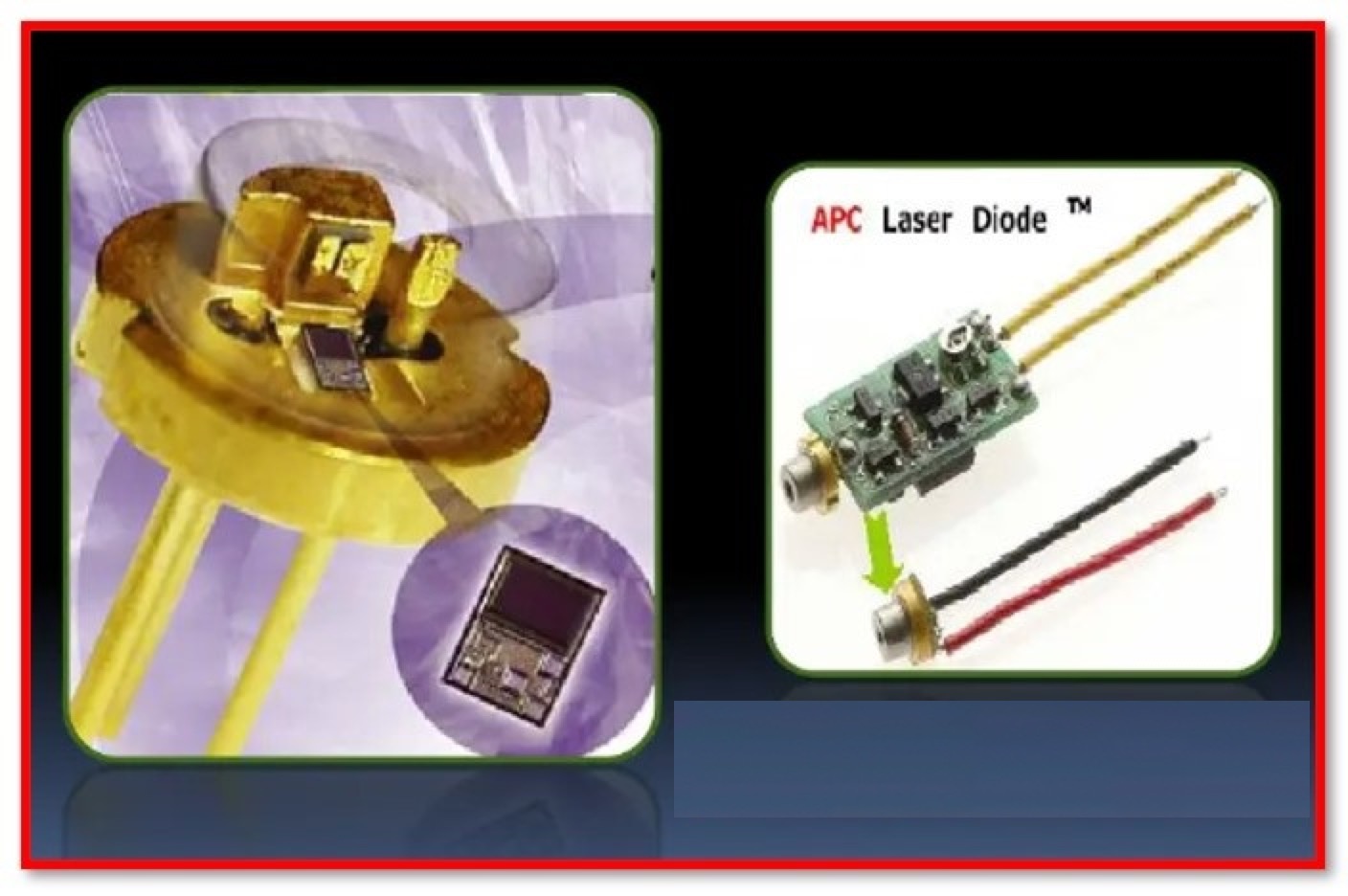
Due to the fact that it generates coherent light, the laser diode does not operate in the same way that a typical LED (light-emitting diode) does. These particular kinds of diodes find widespread use in a variety of domains, including CD drives, DVD players, and laser pointers used in presentations. While these diodes are more affordable than other kinds of laser generators, their cost is much higher when compared to that of LEDs. They also have a limited amount of life.
5). Light Emitting Diode
The phrase light-emitting diode (or) LED refers to one of the most common and widely used varieties of diodes. If the diode is linked such that it has a forwarding bias and then the current will pass through the junction, which will cause the light to be produced. There are several new LED breakthroughs that are converting them into OLEDs and LEDs.
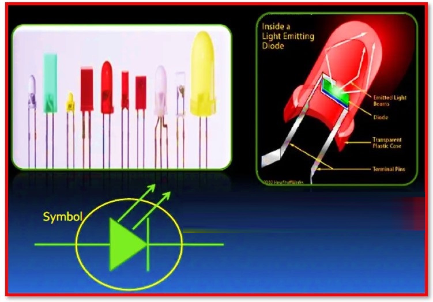
During the forwarding bias working area, this is the sort of diodes that are in operation. There is a flow of the current as soon as the diode begins conducting when we are in this zone. The term “forwarding current” refers to this kind of current. The diode is the source of the light that is produced throughout this operation.
LEDs come in a wide variety of colors. To be more specific, a blinking one that can function as on and off for a predetermined length of time. They may be bicolor leads, in which case two colours are emitted, or they may be tricolour leads, in which case three colours are emitted, depending on the amount of positive voltage received.
In addition to this, there are LEDs that can produce infrared light. Its practical applicability is found in remote controls.
6). Photodiode
Light is sensed by the photodiode in this technique. It has been discovered that the interaction of light with a PN junction may result in the creation of electrons and holes. In most cases, photodiodes function under settings of reverse bias, which allows even a minute quantity of light-induced current flow to be easily detected and monitored. Generating power is another possible use for these kinds of diodes.

Since it is also able to conduct when subjected to reverse bias, the functioning of a photodiode is very similar to that of a zen diode.
Both the value of the current & the light intensity value are directly proportional to one another. They also have reaction times that are sufficiently fast, measuring in nanoseconds rather than milliseconds.
7). PIN Diode
The characteristics of this diode are determined throughout the process of developing it. Both p-type and n-type standards are used in the construction of this type of diode. Th e junction that will be produced as a result of these interactions is known as an intrinsic semiconductor since it will not include any doping concentration.
Applications such as switching may take advantage of having access to this region.
8). Fast Recovery Diode
The diode will have a quicker recovery time. AC is used as the signal input throughout the process of rectification. This levels have both positive and negative aspects. For the polarities to transition from positive to negative (or) from negative to positive, the recovery period must be as short as possible.
When high-frequency applications are being carried out, it is very important to have the quickest possible recovery times. In conditions like these, it is recommended to use this particular diode. As a condition of this, the representation has to be done in an accurate way while still maintaining the signal’s integrity.
9). Step Recovery Diode
It is one of the components of the microwave diode. This often leads to the generation of pulses during the high-frequency range. These diodes are dependent(depending) on type of diodes that have the property of shutting (turning) off quickly due to their operation.
10). Tunnel Diode
These tunnel diodes have been known to require switches while operating in the ultra-high-speed range. The duration of the transition will be measured in nanoseconds or picoseconds. This is used in relaxation oscillator circuits because of the idea of negative resistance that is linked with it.

11). P-N Junction Diode
This is the fundamental diode that is produced when p-type & n-type materials interact with one another. It explores the idea of favouring one viewpoint over another. Because of this biassing, it may function in a variety of modes of operation.
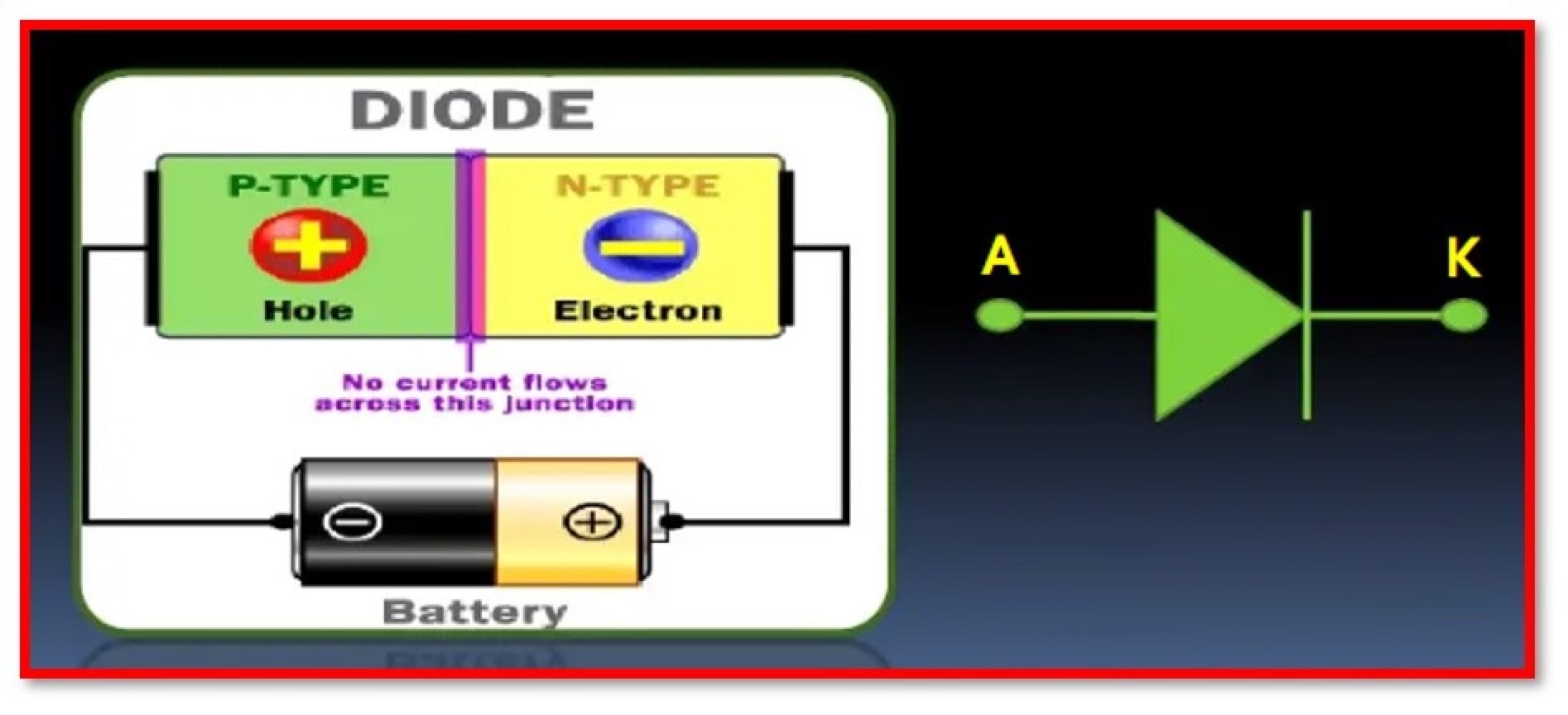
Only when the forwarding bias is applied does this diode conduct. When the bias is in the other direction, there is no clear flow of current. It shows that current is blocked when the bias is in the other direction.
They are used in situations when applications need low currents, such as signal diodes, and are thus favoured. The rectifiers are one of the most fundamental uses for this technology.
12). Zener Diode
It is the kind of diode that has been constructed in such a manner that it is able to function in the reverse-bias mode. When a forward bias is applied, the operating properties of the diode will be comparable to those of a conventional diode that has a p-n junction as its fundamental component.
When the diode is operating in the reverse bias mode, once it has reached the lowest Zener voltage, there will be an increase in the values of the current; however, the voltage will continue to be constant beyond that point.
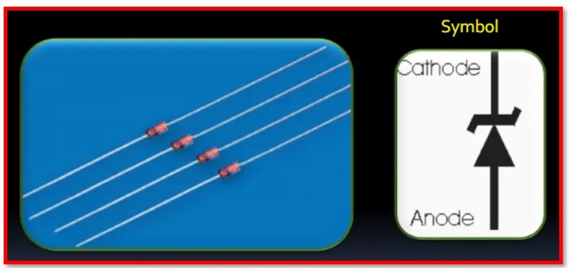
As a result, it may be used in the process of voltage control as a result of this fact. When it begins conducting current under forward bias, the diode has shown its unique ability. The manufacturers determine exactly the more zen voltage will be for this particular kind of diode. Because of this, it is possible to make more zen diodes.
13). Schottky Diodes
A Schottky diode is a kind of diode that is characterised by its ability to perform switching operations at high speeds. Very little voltage loss occurs throughout the forward path, hence this is regarded to be a positive attribute.
Clamping circuits that are quick enough are a good example of where this sort of diode may be made to use, since its uses are readily apparent there. A frequency in the gigahertz range is typical for the operation of diodes of this sort. In other words, it has the potential to be more desirable during high-frequency applications.

14). Shockley Diodes
Switching applications make use of these diodes, which are a different type of diode from the ones described above. It is having some fundamental voltage, also known as trigger voltage, which is present.
It is impossible for this to switch since it will stay in the high resistance mode if the voltage that is provided to it is lower than the basic trigger value. The low resistance route will be constructed as soon as the voltage that is being supplied is greater than the basic trigger value. The Shockley diodes carry out their functions in this manner.
15). Varactor (or) Varicap Diode

This is another unique category of diodes, which occurs when a reverse voltage is applied to the junction of the device. This causes a change in the capacitance of the junction. Since it is a variable capacitance diode, the abbreviation “varicap” might be used to refer to it.

16). Avalanche Diode
The avalanche diode is a kind of reverse bias diode that derives its operation from the avalanche phenomena. The failure of the avalanche occurs when the voltage drop remains constant and is unaffected by the current. Because to the high level of sensitivity that they possess, they are employed for photo-detection.
17). Constant-current Diode
It is an electrical device that restricts current to the maximum value provided. It can also be referred to as a current limiting diode (CLD) (or) a current-regulating diode (CRD) (CRD).
These diodes are made out of an (n-channel)-JFET. The gate is connected to the source and acts as a two terminal current limiter (or) current source. They enable a current to flow through them to a specific value before stopping to increase (develop) further.
18). Gold Doped Diodes
Gold is employed as a dopant in these diodes. Some diodes are more powerful than others. The leakage current at reverse bias is also lower in these diodes. Even with larger voltage drops, the diode can work at signal frequencies. Gold aids in the rapid recombination of the minority carriers in these diodes.
19). Super Barrier Diodes
It is a rectifier diode with a low forward voltage drop as a Schottky diode and a low (reverse) leakage current as a P – N junction diode. It was created for high-power, high-speed switching, and low-loss applications. Super barrier rectifier diodes are the next type of rectifiers that have a lower forward voltage than the Schottky diode.
20). Peltier Diode
It generates heat at two material junction of the semiconductor in this type of diode, which flows from one of the terminal to another terminal. This flow has only one direction, which is the same as in the direction of current flow.
This heat is generated as a result of the electric charge generated by the recombination of the minority charge carriers. This is mostly used for cooling and heating. This sort of diode serves as both a sensor and a heat engine in thermoelectric cooling.
21). Crystal Diode
This is a form of point contact diode that is also known as Cat’s whisker. Its functioning is determined by the contact pressure between the semiconductor crystal & the point.
A metal wire is contained in this, and it is forced against semiconductor crystal. In this condition, the semiconductor crystal serves as the cathode while the metal wire serves as the anode. In nature, these diodes are outdated. Used mostly in microwave receivers & detectors.
22). Vacuum Diodes
Vacuum diodes are made up of two electrodes that serve as an anode and a cathode. Tungsten is used to make the cathode, which emits electrons in a direction of the anode. Electron flow will always go from cathode to anode. As a result, it functions like a switch.
When the cathode is covered with the oxide material, the electron emission capacity is increased. Anodes are rather longer in length, and their surfaces are sometimes roughened to minimise the temperatures that occur in the diode. The diode will only conduct when anode is positive (+) with respect to the cathode terminal.
23). Small Signal Diode
It is a tiny device with disproportional features, primarily used in high frequency and low current application fields such as radios & TVs.
Signal diodes are much smaller than power diodes. One edge is marked with black (or) red to denote the cathode terminal. The performance of the tiny signal diode is particularly effective for applications at high frequencies.
In comparison to their capabilities in other categories, signal diodes typically have a modest current carrying capability and a low power dissipation.They are typically in the range of 150mA & 500mW.
It is used in
Diode applications,
High speed switching,
Parametric amplifiers & many more applications.
24). Large Signal Diode
The PN junction layer on these diodes is rather thick. As a result, they are often utilised in rectification, or converting AC to DC. The big PN Junction boosts the diode’s forward current carrying capability and reverse blocking voltage. Large signal diodes are not appropriate for high-frequency applications.
These diodes are primarily applicable in power supplies like
Rectifiers,
Converter,
Inverters,
Battery charging devicesetc.
The forward resistance of these diodes is a few Ohms, while the reverse blocking resistance is measured in Mega Ohms.
Because of its high current & voltage capability, it may be employed in electrical devices that suppress large peak voltages.
As a result, the many kinds of diodes and the uses for them have been discussed in this post. Each diode has its own one-of-a-kind method of representation, in addition to its own unique method of operation.
Frequently Asked Questions
1). Does a diode convert alternating current(AC) to direct current(DC)?
The diode which enables the current to flow (pass through) in one direction. When utilised with alternating current, the diodes will only conduct for half of the cycle. As a result, they are utilised in the conversion of alternating current to direct current. As a result, diodes are direct current (DC).
2). What is Ideal Diodes?
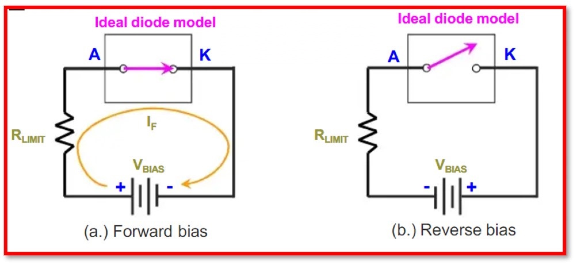
Diodes that are used to regulate the direction of current flow are known as ideal diodes. With an ideal diode, current can only flow in one direction, known as the forward direction, and it cannot flow in the reverse directions.
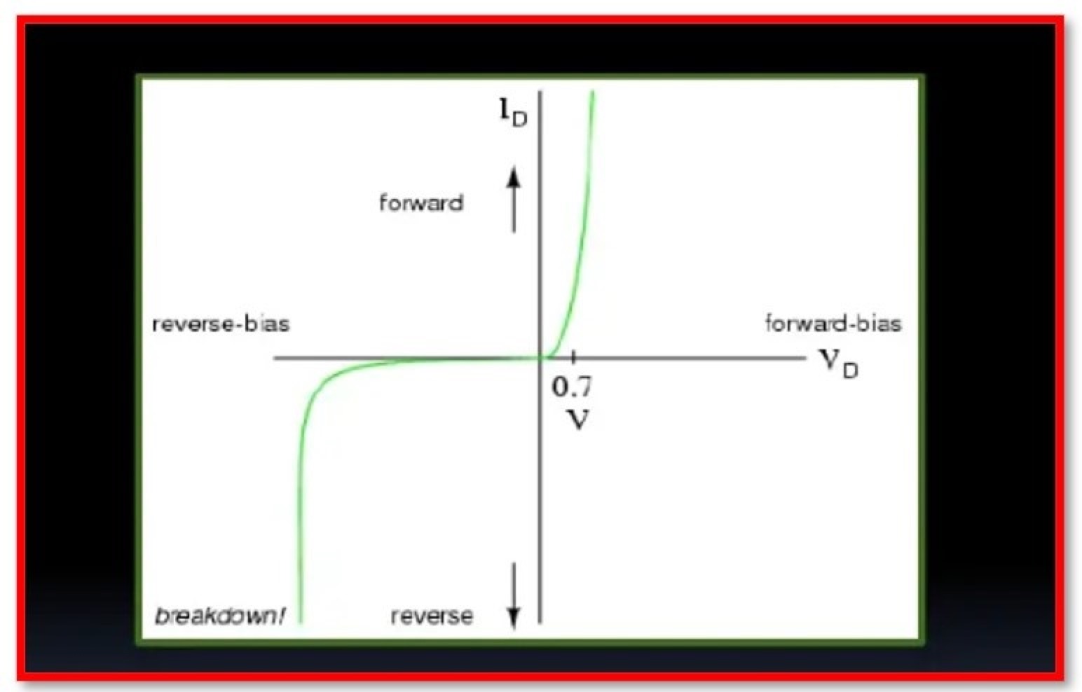
The ideal diodes seem to be an open circuit when they are reverse biassed, and the voltage across is negative in this condition.
3). What is the difference between forward & reverse bias?
Forward biassing happens in a conventional diode when the voltage across the diode allows the normal flow of current, while reverse biassing signifies a voltage across the diode in opposite direction. However , the voltage applied across the diode during reverse biassing does not result in any appreciable current flow.
Statement: Respect the original, good articles worth sharing, if there is infringement please contact delete.
As an electrical engineer with 5 years of experience, I focus on transformer and circuit breaker reliability in 110/33-11kV and 33/11kV substations. I am a professional electrical engineer with experience in transformer service and maintenance.

